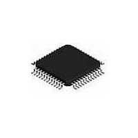
XR16L2750IM-F Exar Corporation, XR16L2750IM-F Datasheet - Page 28

XR16L2750IM-F
Manufacturer Part Number
XR16L2750IM-F
Description
IC UART FIFO 64B DUAL 48TQFP
Manufacturer
Exar Corporation
Type
IrDA or RS- 485r
Datasheet
1.XR16L2750CM-F.pdf
(48 pages)
Specifications of XR16L2750IM-F
Number Of Channels
2, DUART
Package / Case
48-TQFP
Features
*
Fifo's
64 Byte
Protocol
RS232, RS485
Voltage - Supply
2.25 V ~ 5.5 V
With Auto Flow Control
Yes
With Irda Encoder/decoder
Yes
With False Start Bit Detection
Yes
With Modem Control
Yes
With Cmos
Yes
Mounting Type
Surface Mount
Data Rate
6.25 Mbps
Supply Voltage (max)
5.5 V
Supply Voltage (min)
2.25 V
Supply Current
5 mA
Maximum Operating Temperature
+ 85 C
Minimum Operating Temperature
- 40 C
Mounting Style
SMD/SMT
Operating Supply Voltage
2.5 V or 3.3 V or 5 V
No. Of Channels
2
Uart Features
Tx/Rx FIFO Counters
Supply Voltage Range
2.25V To 5.5V
Operating Temperature Range
-40°C To +85°C
Digital Ic Case Style
TQFP
Rohs Compliant
Yes
Lead Free Status / RoHS Status
Lead free / RoHS Compliant
Lead Free Status / RoHS Status
Lead free / RoHS Compliant, Lead free / RoHS Compliant
Other names
1016-1280
Available stocks
Company
Part Number
Manufacturer
Quantity
Price
Company:
Part Number:
XR16L2750IM-F
Manufacturer:
Exar Corporation
Quantity:
10 000
Part Number:
XR16L2750IM-F
Manufacturer:
EXAR/艾科嘉
Quantity:
20 000
XR16L2750
2.25V TO 5.5V DUART WITH 64-BYTE FIFO
LCR[4]: TX and RX Parity Select
If the parity bit is enabled with LCR bit-3 set to a logic 1, LCR BIT-4 selects the even or odd parity format.
•
•
LCR[5]: TX and RX Parity Select
If the parity bit is enabled, LCR BIT-5 selects the forced parity format.
•
•
•
LCR[6]: Transmit Break Enable
When enabled, the Break control bit causes a break condition to be transmitted (the TX output is forced to a
“space", LOW state). This condition remains, until disabled by setting LCR bit-6 to a logic 0.
•
•
LCR[7]: Baud Rate Divisors Enable
Baud rate generator divisor (DLL/DLM) enable.
•
•
The MCR register is used for controlling the serial/modem interface signals or general purpose inputs/outputs.
MCR[0]: DTR# Output
The DTR# pin is a modem control output. If the modem interface is not used, this output may be used as a
general purpose output.
•
•
4.7
Logic 0 = ODD Parity is generated by forcing an odd number of logic 1’s in the transmitted character. The
receiver must be programmed to check the same format (default).
Logic 1 = EVEN Parity is generated by forcing an even number of logic 1’s in the transmitted character. The
receiver must be programmed to check the same format.
LCR BIT-5 = logic 0, parity is not forced (default).
LCR BIT-5 = logic 1 and LCR BIT-4 = logic 0, parity bit is forced to a logical 1 for the transmit and receive
data.
LCR BIT-5 = logic 1 and LCR BIT-4 = logic 1, parity bit is forced to a logical 0 for the transmit and receive
data.
Logic 0 = No TX break condition. (default)
Logic 1 = Forces the transmitter output (TX) to a “space”, LOW, for alerting the remote receiver of a line
break condition.
Logic 0 = Data registers are selected. (default)
Logic 1 = Divisor latch registers are selected.
Logic 0 = Force DTR# output HIGH (default).
Logic 1 = Force DTR# output LOW.
Modem Control Register (MCR) or General Purpose Outputs Control - Read/Write
LCR B
X
0
0
1
1
IT
-5 LCR B
X
0
1
0
1
IT
-4 LCR B
T
ABLE
0
1
1
1
1
11: P
IT
-3
ARITY SELECTION
28
Forced parity to space, “0”
Force parity to mark, “1”
P
ARITY SELECTION
Even parity
Odd parity
No parity
xr
REV. 1.2.1


