ATAKSTK511-3 Atmel, ATAKSTK511-3 Datasheet - Page 19
ATAKSTK511-3
Manufacturer Part Number
ATAKSTK511-3
Description
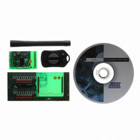
KIT RF MODULE 315MHZ FOR STK500
Manufacturer
Atmel
Series
SmartRF®r
Type
Transmitter, Receiver, ASK, FSKr
Specifications of ATAKSTK511-3
Frequency
433MHz
Wireless Frequency
315 MHz
For Use With/related Products
ATSTK500
Lead Free Status / RoHS Status
Contains lead / RoHS non-compliant
Other names
Q2262874


4.2.3
4.2.4
4.2.5
4.2.6
STK511 User Guide
Configuration Register LED Indicators
DATA Selector Switch
Configure Push Button
On-board Microcontroller
Each configuration register bit has a corresponding LED on the STK511 Receiver Interface Board and is
grouped according to specific functions. If an LED is ON the corresponding bit is set to logic 1. The LEDs
are enclosed by the silkscreen legend and become part of the table for easy reference.
The DATA selector switch controls the routing of the bi-directional DATA line coming from the Receiver
Application Board. The switch either routes the DATA line to the STK511 Receiver Interface Board's on-
board microcontroller or to the Atmel AVR microcontroller on the STK500 board. The silkscreen legend
designates the selected mode based on switch position. To enable the Receiver Application Board, a
low pulse must be applied to the DATA line whenever power is applied (see receiver datasheet “Clearing
the Reset Marker” for more detail). The STK511 Receiver Interface Board provides this signal as part of
the firmware initialization routine. Therefore, when powering up the STK511 Starter Kit and configuring
the registers in the receiver, the DATA Selector Switch must be set to the STK511 position.
Note:
The configuration selected by the DIP switches is not programmed into the receiver until the Configure
button is pressed. When pressed, the on-board microcontroller programs these values into the appropri-
ate registers of the receiver. Each register is written twice to allow verification that the proper data was
set. The button is connected to PB6 of the on-board microcontroller I/O port.
Note:
The STK511 Receiver Interface Board’s on-board microcontroller is the ATmega8515 8-bit AVR. It is
shipped with all of the firmware for supporting the functions of the STK511 Starter Kit. Programming the
flash memory of this microcontroller can be achieved through the STK500.
In order to reprogram the on-board microcontroller through the STK500 complete the following steps:
1. All devices must be removed from the programming sockets on the STK500.
2. Short the ISP Jumper (JP2) on the STK511 Receiver Interface Board.
3. The SPROG3 header on the STK500 must be connected to the ISP6PIN header.
4. The STK511 Receiver Interface Board must be connected through the expansion connectors
The ISP pins are connected to the following I/O pins on the microcontroller.
Table 4-2. STK511 Receiver Interface Board On-board Programming Pinout
(EXPAND0 and EXPAND1).
This is probably the single most important piece of information regarding the successful operation of this
Evaluation Kit. Having this switch in the wrong position can cause a lot of unexplained problems. Always
verify that this switch is set to desired position.
The Data selector switch must first be set to the STK511 position for the settings to be written into the
receiver.
ISP Pin
RST
PB7
PB6
PB5
STK511 Receiver Interface Board
I/O Pin Microcontroller
MOSI
MISO
SCK
RST
4842B–AVR–10/09
4-5
Related parts for ATAKSTK511-3
Image
Part Number
Description
Manufacturer
Datasheet
Request
R

Part Number:
Description:
DEV KIT FOR AVR/AVR32
Manufacturer:
Atmel
Datasheet:

Part Number:
Description:
INTERVAL AND WIPE/WASH WIPER CONTROL IC WITH DELAY
Manufacturer:
ATMEL Corporation
Datasheet:
Part Number:
Description:
Low-Voltage Voice-Switched IC for Hands-Free Operation
Manufacturer:
ATMEL Corporation
Datasheet:
Part Number:
Description:
MONOLITHIC INTEGRATED FEATUREPHONE CIRCUIT
Manufacturer:
ATMEL Corporation
Datasheet:
Part Number:
Description:
AM-FM Receiver IC U4255BM-M
Manufacturer:
ATMEL Corporation
Datasheet:
Part Number:
Description:
Monolithic Integrated Feature Phone Circuit
Manufacturer:
ATMEL Corporation
Datasheet:
Part Number:
Description:
Multistandard Video-IF and Quasi Parallel Sound Processing
Manufacturer:
ATMEL Corporation
Datasheet:
Part Number:
Description:
High-performance EE PLD
Manufacturer:
ATMEL Corporation
Datasheet:
Part Number:
Description:
8-bit Flash Microcontroller
Manufacturer:
ATMEL Corporation
Datasheet:
Part Number:
Description:
2-Wire Serial EEPROM
Manufacturer:
ATMEL Corporation
Datasheet: