ATAKSTK511-3 Atmel, ATAKSTK511-3 Datasheet - Page 20
ATAKSTK511-3
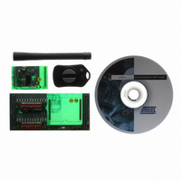
Manufacturer Part Number
ATAKSTK511-3
Description
KIT RF MODULE 315MHZ FOR STK500
Manufacturer
Atmel
Series
SmartRF®r
Type
Transmitter, Receiver, ASK, FSKr
Specifications of ATAKSTK511-3
Frequency
433MHz
Wireless Frequency
315 MHz
For Use With/related Products
ATSTK500
Lead Free Status / RoHS Status
Contains lead / RoHS non-compliant
Other names
Q2262874


4842B–AVR–10/09
STK511 Receiver Interface Board
4.2.7
4.3
4.3.1
4-6
Receive Signal Routing
Software Description
Overview
Two signals from the Receiver Application Board are routed to the STK511 Receiver Interface Board on-
board microcontroller, to allow for operation as a stand-alone system, while the rest are routed to the
STK500. Provisions have been made for re-routing all the signals from the receiver to either the STK511
Receiver Interface Board or the STK500 boards. For the advanced user, this flexibility could be used to
realize a complete stand-alone receiver system. The routing is controlled by selective population of 0-
resistors on the back of the STK511 Receiver Interface Board. The following table lists the routing
choices. Components shown in bold designate how the STK511 Receiver Interface Board is configured
as shipped. To change the signal routing, remove/add the appropriate resistors.
Table 4-3. Receiver Signal Routing
The firmware supplied with the STK511 Receiver Interface Board performs the following functions:
Many Atmel receivers generate a Reset Marker signal, consisting of a 128 kHz square wave, upon
power up. This must be cleared before normal operation can occur. Applying a 10 ms low pulse to the
DATA line clears the Reset Marker. This function is part of the initialization routine of the STK511
Receiver Interface Board firmware. However, the DATA selector switch must be set to STK511 mode
during power up for this to occur.
Clears the Reset Marker upon power up
Reads the values set by the configuration register DIP switches
Programs the OPMODE and LIMIT registers via the bi-directional DATA line
Holds the receiver in a polling mode via the POL/ON line
Pin #
12
11
10
9
8
7
6
5
4
3
2
1
IC_Active
ATA5743
POL/ON
D_CLK
MODE
SENS
DATA
VCC
GND
N/A
U2
IC_ACTIVE
ATA5760/1
POL/ON
D_CLK
V DIV
SENS
DATA
VCC
GND
N/A
ATA5744
ENABLE
DATA
RSSI
VCC
GND
BR0
BR1
N/A
Microcontroller
Routing to
On-board
R32 - NC
R28 - 0
R32 - NC
R29 - 0
R26 - NC
DATA Selector Switch
STK511 User Guide
STK500 Board
Routing to
R31 - 0
R25 - 0
R31 - 0
R27 - NC
R30 - NC
Related parts for ATAKSTK511-3
Image
Part Number
Description
Manufacturer
Datasheet
Request
R

Part Number:
Description:
DEV KIT FOR AVR/AVR32
Manufacturer:
Atmel
Datasheet:

Part Number:
Description:
INTERVAL AND WIPE/WASH WIPER CONTROL IC WITH DELAY
Manufacturer:
ATMEL Corporation
Datasheet:
Part Number:
Description:
Low-Voltage Voice-Switched IC for Hands-Free Operation
Manufacturer:
ATMEL Corporation
Datasheet:
Part Number:
Description:
MONOLITHIC INTEGRATED FEATUREPHONE CIRCUIT
Manufacturer:
ATMEL Corporation
Datasheet:
Part Number:
Description:
AM-FM Receiver IC U4255BM-M
Manufacturer:
ATMEL Corporation
Datasheet:
Part Number:
Description:
Monolithic Integrated Feature Phone Circuit
Manufacturer:
ATMEL Corporation
Datasheet:
Part Number:
Description:
Multistandard Video-IF and Quasi Parallel Sound Processing
Manufacturer:
ATMEL Corporation
Datasheet:
Part Number:
Description:
High-performance EE PLD
Manufacturer:
ATMEL Corporation
Datasheet:
Part Number:
Description:
8-bit Flash Microcontroller
Manufacturer:
ATMEL Corporation
Datasheet:
Part Number:
Description:
2-Wire Serial EEPROM
Manufacturer:
ATMEL Corporation
Datasheet: