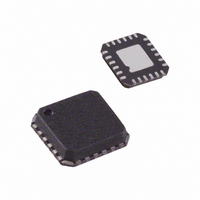
ADL5375-05ACPZ-R7 Analog Devices Inc, ADL5375-05ACPZ-R7 Datasheet - Page 20

ADL5375-05ACPZ-R7
Manufacturer Part Number
ADL5375-05ACPZ-R7
Description
IC MOD QUAD 400MHZ-6GHZ 24LFCSP
Manufacturer
Analog Devices Inc
Datasheet
1.ADL5375-05ACPZ-R7.pdf
(32 pages)
Specifications of ADL5375-05ACPZ-R7
Design Resources
Interfacing ADL5375 to AD9779A Dual-Channel, 1 GSPS High Speed DAC (CN0021) Broadband Low EVM Direct Conversion Transmitter (CN0134)
Function
Modulator
Lo Frequency
400MHz ~ 6GHz
Rf Frequency
400MHz ~ 6GHz
P1db
10.4dBm
Noise Floor
-157.6dBm/Hz
Output Power
1.71dBm
Current - Supply
200mA
Voltage - Supply
4.75 V ~ 5.25 V
Test Frequency
3.5GHz
Package / Case
24-VFQFN, 24-CSP Exposed Pad
Frequency Range
400MHz To 6GHz
Rf Type
Quadrature
Supply Voltage Range
4.75V To 5.25V
Rf Ic Case Style
LFCSP
No. Of Pins
24
Operating Temperature Range
-40°C To +85°C
Frequency Max
6GHz
Lead Free Status / RoHS Status
Lead free / RoHS Compliant
Other names
ADL5375-05ACPZ-R7TR
Available stocks
Company
Part Number
Manufacturer
Quantity
Price
Part Number:
ADL5375-05ACPZ-R7
Manufacturer:
ADI/亚德诺
Quantity:
20 000
ADL5375
BASIC CONNECTIONS
Figure 54 shows the basic connections for the ADL5375.
POWER SUPPLY AND GROUNDING
Pin VPS1 and Pin VPS2 should be connected to the same 5 V
source. Each pin should be decoupled with a 100 pF and
0.1 μF capacitor. These capacitors should be located as close
as possible to the device. The power supply can range between
4.75 V and 5.25 V.
The ten COMM pins should be tied to the same ground plane
through low impedance paths.
The exposed paddle on the underside of the package should also
be soldered to a ground plane with low thermal and electrical
impedance. If the ground plane spans multiple layers on the
circuit board, they should be stitched together with nine vias
under the exposed paddle as illustrated in the Evaluation Board
section. The AN-772 application note discusses the thermal and
electrical grounding of the LFCSP (QFN) package in detail.
BASEBAND INPUTS
The baseband inputs (IBBP, IBBN, QBBP, and QBBN) should be
driven from a differential source. The nominal drive level used
in the characterization of the ADL5375 is 1 V p-p differential
(or 500 mV p-p on each pin).
LOIP
A
VPOS
VPOS
S1
1000pF
1000pF
C6
B
C7
C5
0.1µF
COMM
COMM
DSOP
LOIP
LOIN
NC
Figure 54. Basic Connections for the ADL5375
C3
1000pF
1
2
3
4
5
6
QBBN
IBBN
EXPOSED PADDLE
Rev. A | Page 20 of 32
ADL5375
Z1
All the baseband inputs must be externally dc biased. The
recommended common-mode level is dependent on the
version of the ADL5375.
•
•
LO INPUT
The LO input is designed to be driven from a single-ended
source. The LO source is ac-coupled through a series capacitor
to the LOIP pin while the LOIN pin is ac-coupled to ground
through a second capacitor.
The typical LO drive level, which was used for the
characterization of the ADL5375, is 0 dBm.
Differential operation is also possible, in which case both sides
of the differential LO source should be ac-coupled through a
pair of series capacitors to the LOIP and LOIN pins.
RF OUTPUT
The RF output is available at the RFOUT pin (Pin 16), which can
drive a 50 Ω load. The internal balun provides a low dc path to
ground. In most situations, the RFOUT pin must be ac-coupled
to the load.
IBBP
QBBP
ADL5375-05: 500 mV
ADL5375-15: 1500 mV
18
17
16
15
14
13
VPS1
COMM
RFOUT
NC
COMM
NC
1000pF
1000pF
C2
C1
GND
0.1µF
C4
RFOUT
VPOS


