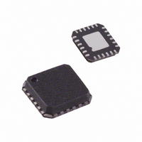
ADL5375-05ACPZ-R7 Analog Devices Inc, ADL5375-05ACPZ-R7 Datasheet - Page 22

ADL5375-05ACPZ-R7
Manufacturer Part Number
ADL5375-05ACPZ-R7
Description
IC MOD QUAD 400MHZ-6GHZ 24LFCSP
Manufacturer
Analog Devices Inc
Datasheet
1.ADL5375-05ACPZ-R7.pdf
(32 pages)
Specifications of ADL5375-05ACPZ-R7
Design Resources
Interfacing ADL5375 to AD9779A Dual-Channel, 1 GSPS High Speed DAC (CN0021) Broadband Low EVM Direct Conversion Transmitter (CN0134)
Function
Modulator
Lo Frequency
400MHz ~ 6GHz
Rf Frequency
400MHz ~ 6GHz
P1db
10.4dBm
Noise Floor
-157.6dBm/Hz
Output Power
1.71dBm
Current - Supply
200mA
Voltage - Supply
4.75 V ~ 5.25 V
Test Frequency
3.5GHz
Package / Case
24-VFQFN, 24-CSP Exposed Pad
Frequency Range
400MHz To 6GHz
Rf Type
Quadrature
Supply Voltage Range
4.75V To 5.25V
Rf Ic Case Style
LFCSP
No. Of Pins
24
Operating Temperature Range
-40°C To +85°C
Frequency Max
6GHz
Lead Free Status / RoHS Status
Lead free / RoHS Compliant
Other names
ADL5375-05ACPZ-R7TR
Available stocks
Company
Part Number
Manufacturer
Quantity
Price
Part Number:
ADL5375-05ACPZ-R7
Manufacturer:
ADI/亚德诺
Quantity:
20 000
ADL5375
OPTIMIZATION
The carrier feedthrough and sideband suppression performance of
the ADL5375 can be improved by using optimization techniques.
Carrier Feedthrough Nulling
Carrier feedthrough results from minute dc offsets that occur
between each of the differential baseband inputs. In an ideal
modulator, the quantities (V
are equal to zero, which results in no carrier feedthrough. In a real
modulator, those two quantities are nonzero and, when mixed
with the LO, result in a finite amount of carrier feedthrough. The
ADL5375 is designed to provide a minimal amount of carrier
feedthrough. Should even lower carrier feedthrough levels be
required, minor adjustments can be made to the (V
and (V
while the Q-channel offset is varied until a minimum carrier
feedthrough level is obtained. The Q-channel offset required to
achieve this minimum is held constant, while the offset on the
I-channel is adjusted until a new minimum is reached. Through
two iterations of this process, the carrier feedthrough can be
reduced to as low as the output noise. The ability to null is
sometimes limited by the resolution of the offset adjustment.
Figure 55 illustrates the typical relationship between carrier
feedthrough and dc offset around the null.
Using the ADL5375-05 version as an example, note that
throughout the nulling process, the dc bias for the base-
band inputs remains at 500 mV. When no offset is applied,
When an offset of +V
Figure 55. Example of Typical Carrier Feedthrough vs. DC Offset Voltage
V
V
V
V
V
IBBP
IBBP
IBBP
IBBN
IBBP
QBBP
–60
–64
–68
–72
–76
–80
–84
–88
–300 –240 –180 –120
= V
− V
= 500 mV + V
− V
= 500 mV − V
− V
IBBN
IBBN
IBBN
QBBN
= 500 mV, or
= V
= V
) offsets. The I-channel offset is held constant,
IOS
IOS
IOS
= 0 V
IOS
is applied to the I-channel inputs,
IOS
V
/2, and
/2, such that
P
–60
IBBP
– V
N
− V
OFFSET (µV)
0
IBBN
60
) and (V
120
180
QBBP
IBBP
− V
240
− V
QBBN
300
IBBN
)
Rev. A | Page 22 of 32
)
The same applies to the Q-channel. For the ADL5375-15, the
same theory applies except that
It is often desirable to perform a one-time carrier null calibra-
tion. This is usually performed at a given frequency and the
radio allowed to operate over a frequency range on each side
of that frequency. The nulled carrier feedthrough level degrades
somewhat as the LO frequency is moved away from the
frequency at which the null was performed. This variation is
very small across a 30 MHz or 60 MHz cellular band, however.
This small variation is due to the effects of LO-to-RF output
leakage around the package and on the board as the frequency
changes. Despite the degradation, the LO leakage can be
expected to be better than when no nulling is performed.
Sideband Suppression Optimization
Sideband suppression results from relative gain and relative
phase offsets between the I-channel and Q-channel and can
be suppressed through adjustments to those two parameters.
Figure 56 illustrates how sideband suppression is affected by
the gain and phase imbalances.
Figure 56 underlines the fact that adjusting only one parameter
improves the sideband suppression only to a point, unless the
other parameter is also adjusted. For example, if the amplitude
offset is 0.25 dB, improving the phase imbalance by better than
1° does not yield any improvement in the sideband suppression.
For optimum sideband suppression, an iterative adjustment
between phase and amplitude is required.
The sideband suppression nulling can be performed either
through adjusting the gain for each channel or through the
modification of the phase and gain of the digital data coming
from the baseband signal processor.
V
Figure 56. Sideband Suppression vs. Quadrature Phase Error for
IBBP
–10
–20
–30
–40
–50
–60
–70
–80
–90
0
0.01
= V
2.5dB
1.25dB
0.5dB
0.25dB
0.125dB
0.05dB
0.025dB
0.0125dB
0dB
IBBN
Various Quadrature Amplitude Offsets
= 1500 mV.
0.1
PHASE ERROR (Degrees)
1
10
100


