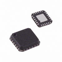
ADL5375-05ACPZ-R7 Analog Devices Inc, ADL5375-05ACPZ-R7 Datasheet - Page 3

ADL5375-05ACPZ-R7
Manufacturer Part Number
ADL5375-05ACPZ-R7
Description
IC MOD QUAD 400MHZ-6GHZ 24LFCSP
Manufacturer
Analog Devices Inc
Datasheet
1.ADL5375-05ACPZ-R7.pdf
(32 pages)
Specifications of ADL5375-05ACPZ-R7
Design Resources
Interfacing ADL5375 to AD9779A Dual-Channel, 1 GSPS High Speed DAC (CN0021) Broadband Low EVM Direct Conversion Transmitter (CN0134)
Function
Modulator
Lo Frequency
400MHz ~ 6GHz
Rf Frequency
400MHz ~ 6GHz
P1db
10.4dBm
Noise Floor
-157.6dBm/Hz
Output Power
1.71dBm
Current - Supply
200mA
Voltage - Supply
4.75 V ~ 5.25 V
Test Frequency
3.5GHz
Package / Case
24-VFQFN, 24-CSP Exposed Pad
Frequency Range
400MHz To 6GHz
Rf Type
Quadrature
Supply Voltage Range
4.75V To 5.25V
Rf Ic Case Style
LFCSP
No. Of Pins
24
Operating Temperature Range
-40°C To +85°C
Frequency Max
6GHz
Lead Free Status / RoHS Status
Lead free / RoHS Compliant
Other names
ADL5375-05ACPZ-R7TR
Available stocks
Company
Part Number
Manufacturer
Quantity
Price
Part Number:
ADL5375-05ACPZ-R7
Manufacturer:
ADI/亚德诺
Quantity:
20 000
SPECIFICATIONS
V
500 mV (ADL5375-05) or 1500 mV (ADL5375-15) dc bias; baseband I/Q frequency (f
Table 1.
Parameter
OPERATING FREQUENCY RANGE
LO = 450 MHz
LO = 900 MHz
S
Low frequency
High frequency
Output Power, P
Modulator Voltage Gain
Output P1dB
Output Return Loss
Carrier Feedthrough
Sideband Suppression
Quadrature Error
I/Q Amplitude Balance
Second Harmonic
Third Harmonic
Output IP2
Output IP3
Noise Floor
Output Power, P
Modulator Voltage Gain
Output P1dB
Output Return Loss
Carrier Feedthrough
Sideband Suppression
Quadrature Error
I/Q Amplitude Balance
Second Harmonic
Third Harmonic
Output IP2
Output IP3
Noise Floor
= 5 V; T
ADL5375-05
ADL5375-15
ADL5375-05
ADL5375-15
ADL5375-05
ADL5375-15
ADL5375-05
ADL5375-15
A
= 25°C; LO = 0 dBm single-ended drive; baseband I/Q amplitude = 1 V p-p differential sine waves in quadrature with a
OUT
OUT
Conditions
V
RF output divided by baseband input voltage
P
P
P
P
f1
P
f1
P
I/Q inputs = 0 V differential with a dc bias
only, 20 MHz carrier offset
V
RF output divided by baseband input voltage
P
P
f1
P
f1
P
I/Q inputs = 0 V differential with a dc bias
only, 20 MHz carrier offset
P
P
P
P
P
P
IQ
OUT
OUT
OUT
OUT
OUT
OUT
IQ
OUT
OUT
OUT
OUT
OUT
OUT
OUT
OUT
OUT
OUT
BB
BB
BB
BB
= 1 V p-p differential
= 1 V p-p differential
= 3.5 MHz, f2
= 3.5 MHz, f2
= 3.5 MHz, f2
= 3.5 MHz, f2
≈ −5 dBm @ f
− (f
= 0.46 dBm
− (f
= 0.87 dBm
= 0.46 dBm
≈ −5 dBm @ f
≈ −5 dBm @ f
− (f
= 0.47 dBm
− (f
= 0.47 dBm
≈ −5 dBm @ f
= 0.87 dBm
= 0.87 dBm
= 0.87 dBm
LO
LO
LO
LO
+ (2 × f
+ (3 × f
+ (2 × f
+ (3 × f
BB
BB
BB
BB
BB
BB
BB
BB
LO
LO
LO
LO
))
))
))
))
= 4.5 MHz,
= 4.5 MHz,
= 4.5 MHz,
= 4.5 MHz,
= 900 MHz
= 900 MHz
= 900 MHz
= 900 MHz
Rev. A | Page 3 of 32
Min
ADL5375-05
BB
) = 1 MHz, unless otherwise noted.
Typ
400
6000
0.87
−3.1
9.4
−14.7
−48.0
−33.1
2.52
−0.05
−74.5
−51.3
65.0
28.1
−160.5
0.87
−3.1
9.4
−14.1
−46.2
−52.1
−0.29
−0.05
−73.3
−51.5
68.3
26.8
−160.0
Max
Min
ADL5375-15
Typ
400
6000
0.46
−3.5
9.9
−14.7
−52.2
−35.5
1.64
−0.07
−74.5
−77.1
67.9
23.0
−157.0
0.47
−3.5
9.9
−14.1
−46.2
−50.4
−0.37
−0.07
−73
−71
66.2
22.9
−157.1
Max
ADL5375
Unit
MHz
MHz
dBm
dB
dBm
dB
dBm
dBc
Degrees
dB
dBc
dBc
dBm
dBm
dBm/Hz
dBm
dB
dBm
dB
dBm
dBc
Degrees
dB
dBc
dBc
dBm
dBm
dBm/Hz


