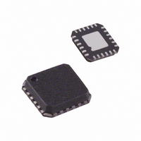
ADL5375-05ACPZ-R7 Analog Devices Inc, ADL5375-05ACPZ-R7 Datasheet - Page 24

ADL5375-05ACPZ-R7
Manufacturer Part Number
ADL5375-05ACPZ-R7
Description
IC MOD QUAD 400MHZ-6GHZ 24LFCSP
Manufacturer
Analog Devices Inc
Datasheet
1.ADL5375-05ACPZ-R7.pdf
(32 pages)
Specifications of ADL5375-05ACPZ-R7
Design Resources
Interfacing ADL5375 to AD9779A Dual-Channel, 1 GSPS High Speed DAC (CN0021) Broadband Low EVM Direct Conversion Transmitter (CN0134)
Function
Modulator
Lo Frequency
400MHz ~ 6GHz
Rf Frequency
400MHz ~ 6GHz
P1db
10.4dBm
Noise Floor
-157.6dBm/Hz
Output Power
1.71dBm
Current - Supply
200mA
Voltage - Supply
4.75 V ~ 5.25 V
Test Frequency
3.5GHz
Package / Case
24-VFQFN, 24-CSP Exposed Pad
Frequency Range
400MHz To 6GHz
Rf Type
Quadrature
Supply Voltage Range
4.75V To 5.25V
Rf Ic Case Style
LFCSP
No. Of Pins
24
Operating Temperature Range
-40°C To +85°C
Frequency Max
6GHz
Lead Free Status / RoHS Status
Lead free / RoHS Compliant
Other names
ADL5375-05ACPZ-R7TR
Available stocks
Company
Part Number
Manufacturer
Quantity
Price
Part Number:
ADL5375-05ACPZ-R7
Manufacturer:
ADI/亚德诺
Quantity:
20 000
ADL5375
Driving the ADL5375-15 with a TXDAC
The ADL5375-15 requires a 1500 mV dc bias and therefore
requires a slightly more complex interface that performs a dc
level shift on the baseband signals. It is necessary to level-shift
the DAC output from a 500 mV dc bias to the 1500 mV dc bias
that the ADL5375-15 requires.
Level-shifting can be achieved with either a passive network
or an active circuit. A passive network of resistors is shown
in Figure 62. In this network, the dc bias of the DAC remains
at 500 mV while the input to the ADL5375-15 is 1500 mV.
It should be noted that this passive level-shifting network
introduces approximately 2 dB of loss in the ac signal.
AD9779A
OUT1_P
OUT1_N
OUT2_N
OUT2_P
–10
–20
–30
–40
–50
–60
Figure 61. Frequency Response for DAC Modulator Interface with
0
1
92
93
84
83
RBQN
RBQP
RBIN
RBIP
50Ω
50Ω
50Ω
50Ω
Figure 60. DAC Modulator Interface with
10 MHz Third-Order, Bessel Filter
10 MHz Third-Orde,r Bessel Filter
53.62nF
53.62nF
GROUP DELAY
C1Q
C1I
FREQUENCY (MHz)
771.1nH
771.1nH
771.1nH
771.1nH
350.1pF
350.1pF
LNQ
LPQ
10
LPI
LNI
C2Q
C2I
MAGNITUDE
RSLQ
100Ω
100Ω
RSLI
21
22
10
9
ADL5375-05
IBBP
IBBN
QBBN
QBBP
100
36
30
24
18
12
6
0
Rev. A | Page 24 of 32
The active level shifting circuit involves the use of the
dual-differential amplifier. This device has a VOCM pin that
sets the output dc bias. Through this pin, the output common-
mode of the amplifier can be easily set to the requisite 1.5 V for
biasing the ADL5375-15 baseband inputs.
USING THE AD9779A AUXILIARY DAC FOR
CARRIER FEEDTHROUGH NULLING
The AD9779A features an auxiliary DAC that can be used to
inject small currents into the differential outputs for each
main DAC channel. This feature can be used to produce the
small offset voltages necessary to null out the carrier feed-
through from the modulator. Figure 63 shows the interface
required to use the auxiliary DACs, which adds four resistors
to the interface.
AD9779A
AD9779A
OUT1_N
AUX1_N
AUX2_N
OUT2_N
AUX1_P
OUT1_P
OUT2_P
AUX2_P
OUT1_P
OUT1_N
OUT2_N
OUT2_P
Figure 62. Passive Level-Shifting Network For Biasing ADL5375-15
Figure 63. DAC Modulator Interface with Auxiliary DAC Resistors
500Ω
500Ω
500Ω
500Ω
90
93
92
89
87
84
83
86
93
92
84
83
RBQN
RBQP
RBIP
RBIN
50Ω
50Ω
50Ω
50Ω
RBQN
RBQP
45.3Ω
45.3Ω
45.3Ω
45.3Ω
RBIN
RBIP
53.62nF
250Ω
250Ω
250Ω
250Ω
53.62nF
C1Q
C1I
RSQN
RSQP
RSIN
RSIP
1kΩ
1kΩ
1kΩ
1kΩ
from TxDAC
771.1nH
771.1nH
771.1nH
771.1nH
350.1pF
350.1pF
LNQ
LPQ
LPI
LNI
C2Q
C2I
3480Ω
3480Ω
3480Ω
3480Ω
RLQN
RLQP
RLIN
RLIP
RSLQ
100Ω
100Ω
RSLI
5V
5V
21
22
10
10
21
22
9
9
ADL5375-15
ADL5375-05
IBBP
IBBN
QBBN
QBBP
IBBP
IBBN
QBBN
QBBP
ADA4938


