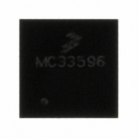
MC33596FCE Freescale Semiconductor, MC33596FCE Datasheet - Page 27

MC33596FCE
Manufacturer Part Number
MC33596FCE
Description
IC RECEIVER UHF PLL TUNED 32-QFN
Manufacturer
Freescale Semiconductor
Type
Receiverr
Datasheet
1.MC33596FCAE.pdf
(70 pages)
Specifications of MC33596FCE
Frequency
304, 315, 426, 434, 868 & 915MHz
Sensitivity
-104dBm
Data Rate - Maximum
22.4 kBaud
Modulation Or Protocol
FSK, OOK
Applications
General Data Transfer
Current - Receiving
10.3mA
Data Interface
PCB, Surface Mount
Antenna Connector
PCB, Surface Mount
Voltage - Supply
2.7 V ~ 3.6 V, 4.5 V ~ 5.5 V
Operating Temperature
-40°C ~ 85°C
Package / Case
32-QFN
Operating Frequency
915 MHz
Operating Supply Voltage
3.3 V or 5 V
Maximum Operating Temperature
+ 85 C
Minimum Operating Temperature
- 40 C
Mounting Style
SMD/SMT
Lead Free Status / RoHS Status
Request inventory verification / Request inventory verification
Features
-
Memory Size
-
Lead Free Status / Rohs Status
Lead free / RoHS Compliant
13.2 State Machine
The configuration mode is selected by the microcontroller unit (MCU) to write to the internal registers (to
configure the system) or to read them. In this mode, the SPI is a slave. The analog parts (receiver) remain
in the state (on, off) they were in prior to entering configuration mode, until a new configuration changes
them. In configuration mode, data can not be received. As long as a low level is applied to CONFB, the
circuit stays in State 1, the only state in this mode.
Figure 21
configuration mode. SPI startup time corresponds to the addition of the crystal oscillator lock time
(parameter 5.10) and the PLL lock time (parameter 5.9).
Freescale Semiconductor
STROBE
STROBE
STROBE
(Output)
(Output)
CONFB
CONFB
CONFB
(Output)
(Input)
(Input)
(Input)
(Input)
SCLK
SCLK
(Input)
MOSI
MOSI
MISO
MISO
(Input)
SCLK
MOSI
MISO
SEB
SEB
SEB
1
1
0
0
1
1
0
0
1
1
0
0
1
1
0
0
1
1
0
0
1
1
0
0
1
0
1
0
1
0
1
0
1
0
1
0
describe the valid sequence for enabling a correct transition from Standby/LVD mode to
A low level applied to CONFB and a high level to STROBE do not affect
the configuration register contents.
N1 N0 A4 A3 A2 A1 A0 R/W
N1 N0 A4 A3 A2 A1 A0 R/W
N1 N0 A4 A3 A2 A1 A0 R/W
Figure 19. Write Operation in Configuration Mode (N[1:0] = 01)
Figure 20. Read Operation in Configuration Mode (N[1:0] = 01)
MC33596 Data Sheet, Rev. 4
D7 D6 D5 D4 D3 D2 D1 D0
D7 D6 D5 D4 D3 D2 D1 D0
D7 D6 D5 D4 D3 D2 D1
NOTE
D0
D7 D6 D5 D4 D3 D2 D1 D0
D7 D6 D5 D4 D3 D2 D1 D0
D7 D6 D5 D4 D3 D2 D1 D0
Configuration Mode
27


