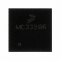
MC33596FCE Freescale Semiconductor, MC33596FCE Datasheet - Page 6

MC33596FCE
Manufacturer Part Number
MC33596FCE
Description
IC RECEIVER UHF PLL TUNED 32-QFN
Manufacturer
Freescale Semiconductor
Type
Receiverr
Datasheet
1.MC33596FCAE.pdf
(70 pages)
Specifications of MC33596FCE
Frequency
304, 315, 426, 434, 868 & 915MHz
Sensitivity
-104dBm
Data Rate - Maximum
22.4 kBaud
Modulation Or Protocol
FSK, OOK
Applications
General Data Transfer
Current - Receiving
10.3mA
Data Interface
PCB, Surface Mount
Antenna Connector
PCB, Surface Mount
Voltage - Supply
2.7 V ~ 3.6 V, 4.5 V ~ 5.5 V
Operating Temperature
-40°C ~ 85°C
Package / Case
32-QFN
Operating Frequency
915 MHz
Operating Supply Voltage
3.3 V or 5 V
Maximum Operating Temperature
+ 85 C
Minimum Operating Temperature
- 40 C
Mounting Style
SMD/SMT
Lead Free Status / RoHS Status
Request inventory verification / Request inventory verification
Features
-
Memory Size
-
Lead Free Status / Rohs Status
Lead free / RoHS Compliant
NOTES:
1
Power Supply
5
The circuit can be supplied from a 3 V voltage regulator or battery cell by connecting VCCIN,
VCCINOUT, and VCCDIG (See
connected to VCCIN; in this case VCCINOUT and VCCDIG should not be connected to VCCIN (See
Figure 41
An on-chip low drop-out voltage regulator supplies the RF and analog modules (except the strobe
oscillator and the low voltage detector, which are directly supplied from VCCINOUT). This voltage
regulator is supplied from pin VCCINOUT and its output is connected to VCC2OUT. An external
capacitor (C8 = 100 nF) must be inserted between VCC2OUT and GND for stabilization and decoupling.
The analog and RF modules must be supplied by VCC2 by externally wiring VCC2OUT to VCC2IN,
VCC2RF, and VCC2VCO.
A second voltage regulator supplies the digital part. This regulator is powered from pin VCCDIG and its
output is connected to VCCDIG2. An external capacitor (C10 = 100 nF) must be inserted between
VCCDIG2 and GNDDIG, for decoupling. The supply voltage VCCDIG2 is equal to 1.6 V. In standby
mode, this voltage regulator goes into an ultra-low-power mode, but VCCDIG2 = 0.7 × V
This enables the internal registers to be supplied, allowing configuration data to be saved.
6
At power-on, an internal reset signal (Power-on Reset, POR) is generated when supply voltage is around
1.3 V. All registers are reset.
When the LVDE bit is set, the low-voltage detection module is enabled. This block compares the supply
voltage on VCCINOUT with a reference level of about 1.8 V. If the voltage on VCCINOUT drops below
1.8 V, status bit LVDS is set. The information in status bit LVDS is latched and reset after a read access.
6
Supply voltage on VCCIN, VCCINOUT, VCCDIG for 3 V operation
Supply voltage on VCCIN for 5 V operation
–40°C to +85°C: MC33596FCE/FJE.
–20°C to +85°C: MC33596FCAE/FJAE.
Power Supply
Supply Voltage Monitoring and Reset
or
Figure
If LVDE = 1, the LVD module remains enabled. The circuit cannot be put
in standby mode, but remains in LVD mode with a higher quiescent current,
due to the monitoring circuitry. LVD function is not accurate in standby
mode.
42).
Table 3. Supply Voltage Range Versus Ambient Temperature
Parameter
Figure 43
MC33596 Data Sheet, Rev. 4
or
Figure
NOTE
44). It is also possible to use a 5 V power supply
Symbol
V
V
CC3V
CC5V
–40°C to +85°C
2.7 to 3.6
4.5 to 5.5
Temperature Range
–20°C to +85°C
Freescale Semiconductor
2.1 to 3.6
4.5 to 5.5
CCDIG.
1
Unit
V
V


