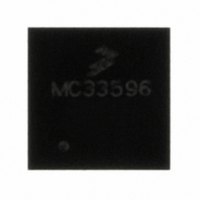
MC33596FCE Freescale Semiconductor, MC33596FCE Datasheet - Page 42

MC33596FCE
Manufacturer Part Number
MC33596FCE
Description
IC RECEIVER UHF PLL TUNED 32-QFN
Manufacturer
Freescale Semiconductor
Type
Receiverr
Datasheet
1.MC33596FCAE.pdf
(70 pages)
Specifications of MC33596FCE
Frequency
304, 315, 426, 434, 868 & 915MHz
Sensitivity
-104dBm
Data Rate - Maximum
22.4 kBaud
Modulation Or Protocol
FSK, OOK
Applications
General Data Transfer
Current - Receiving
10.3mA
Data Interface
PCB, Surface Mount
Antenna Connector
PCB, Surface Mount
Voltage - Supply
2.7 V ~ 3.6 V, 4.5 V ~ 5.5 V
Operating Temperature
-40°C ~ 85°C
Package / Case
32-QFN
Operating Frequency
915 MHz
Operating Supply Voltage
3.3 V or 5 V
Maximum Operating Temperature
+ 85 C
Minimum Operating Temperature
- 40 C
Mounting Style
SMD/SMT
Lead Free Status / RoHS Status
Request inventory verification / Request inventory verification
Features
-
Memory Size
-
Lead Free Status / Rohs Status
Lead free / RoHS Compliant
Bank Access and Register Mapping
Bits RSSI[3:0] contain the result of the analog-to-digital conversion of the signal measured at the IF filter
output.
17
Registers are physically mapped following a byte organization. The possible address space is 32 bytes. The
base address is specified in the command byte. This is then incremented internally to address each register,
up to the number of registers specified by N[1:0], also specified by this command byte. All registers can
then be scanned, whatever the type of transmission (read or write); however, writing to read-only bits or
registers has no effect. When the last implemented address is reached, the internal address counter
automatically loops back to the first mapped address ($00).
At any time, it is possible to write or read the content of any register of Bank A and Bank B. Register access
is defined as follows:
42
R/W
R
RR
R [A]
RR [A]
RESET
Bank Access and Register Mapping
RSSIx
LDVS
SOE
OLS
Bit
Bit can be read and written.
Bit can be read. Write has no effect on bit value.
Bit can be read. Read or write resets the value.
Bit can be read. This returns the same value as Bank A.
Bit can be read. This returns the same value as Bank A. Read or write resets the value.
Bank
A, B
A, B
A, B
A, B
A
CONFIG1
CONFIG3
CONFIG3
CONFIG2
RSSI
Byte
Table 20. Access to Specific Bits
MC33596 Data Sheet, Rev. 4
RR-RR[A}
R/W-R[A}
Access
R-R[A]
R-R[A}
R/W
Available in BANKA.
Bit value is the real time status of the PLL, BANKA,
and BANKB access reflect the same value.
Bit value is the latched value of the low-voltage
detector. Read or write from any bank resets value.
SOE can be modified in BANKA. Access from BANKB
reflects BANKA value.
RSSI value is directly read from RSSI converter.
Reflected value is the same whatever the active byte.
Comment
Freescale Semiconductor


