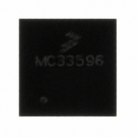
MC33596FCE Freescale Semiconductor, MC33596FCE Datasheet - Page 9

MC33596FCE
Manufacturer Part Number
MC33596FCE
Description
IC RECEIVER UHF PLL TUNED 32-QFN
Manufacturer
Freescale Semiconductor
Type
Receiverr
Datasheet
1.MC33596FCAE.pdf
(70 pages)
Specifications of MC33596FCE
Frequency
304, 315, 426, 434, 868 & 915MHz
Sensitivity
-104dBm
Data Rate - Maximum
22.4 kBaud
Modulation Or Protocol
FSK, OOK
Applications
General Data Transfer
Current - Receiving
10.3mA
Data Interface
PCB, Surface Mount
Antenna Connector
PCB, Surface Mount
Voltage - Supply
2.7 V ~ 3.6 V, 4.5 V ~ 5.5 V
Operating Temperature
-40°C ~ 85°C
Package / Case
32-QFN
Operating Frequency
915 MHz
Operating Supply Voltage
3.3 V or 5 V
Maximum Operating Temperature
+ 85 C
Minimum Operating Temperature
- 40 C
Mounting Style
SMD/SMT
Lead Free Status / RoHS Status
Request inventory verification / Request inventory verification
Features
-
Memory Size
-
Lead Free Status / Rohs Status
Lead free / RoHS Compliant
9
The MC33596 and the MCU communicate via a serial peripheral interface (SPI). According to the selected
mode, the MC33596 or the MCU manages the data transfer. The MC33596’s digital interface can be used
as a standard SPI (master/slave) or as a simple interface (SPI deselected). In the following case, the
interface’s pins are used as standard I/O pins. However, the MCU has the highest priority, as it can control
the MC33596 by setting CONFB pin to the low level. During an SPI access, the STROBE pin must remain
at high level to prevent the MC33596 from entering standby mode.
The interface is operated by six I/O pins.
Table 5
Freescale Semiconductor
•
•
•
•
•
•
•
In direct access, the user programs direct all three frequency registers.
CONFB — Configuration control input
The configuration mode is reached by setting CONFB to low level.
STROBE — Wakeup control input
The STROBE pin controls the ON/OFF sequence of the MC33596. When STROBE is set to low
level, the receiver is off—when STROBE is set to high level, the receiver is on. The current
consumption in receive mode can be reduced by strobing the receiver. The periodic wakeup can be
done by MCU only or by an internal oscillator thanks to an external capacitor (strobe oscillator
must be previously enabled by setting SOE bit to 1). Refer to
Control,” for more details.
SEB — Serial interface enable control input
When SEB is set high, pins SCLK, MOSI, and MISO are set to high impedance, and the SPI bus
is disabled. When SEB is set low, SPI bus is enabled. This allows individual selection in a multiple
device system, where all devices are connected via the same bus. The rest of the circuit remains in
the current state, enabling fast recovery times.
If the MCU shares the SPI access with the MC33596 only, SEB control by the MCU is optional.
If not used, it could be hardwired to 0.
SCLK — Serial clock input/output
Synchronizes data movement in and out of the device through its MOSI and MISO lines. The
master and slave devices can exchange a byte of information during a sequence of eight clock
cycles. Since SCLK is generated by the master device, this line is an input on the slave device.
MOSI — Master output slave input/output
In configuration mode, MOSI is an input.
In receive mode, MOSI is an output. Received data is sent on MOSI (see
When no data are output, SCLK and MOSI force a low level.
MISO — Master input/slave output
In configuration mode only, data read from registers is sent to the MCU with the MSB first. There
is no master function. Data are valid on falling edges of SCLK. This means that the clock phase
and polarity control bits of the microcontroller SPI have to be CPOL = 0 and CPHA = 1 (using
Freescale acronyms).
summarizes the serial digital interface feature versus the selected mode.
MCU Interface
MC33596 Data Sheet, Rev. 4
Section 11.3, “Receiver On/Off
Table
5).
MCU Interface
9


