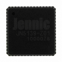
JN5139-Z01-V NXP Semiconductors, JN5139-Z01-V Datasheet - Page 15

JN5139-Z01-V
Manufacturer Part Number
JN5139-Z01-V
Description
IC MCU ZIGBEE 32BIT 2.4G 56QFN
Manufacturer
NXP Semiconductors
Series
JN5139-Z01Rxr
Specifications of JN5139-Z01-V
Frequency
2.4GHz
Modulation Or Protocol
802.15.4 Zigbee
Applications
General Purpose
Power - Output
3dBm
Sensitivity
-97dBm
Voltage - Supply
2.2 V ~ 3.6 V
Current - Receiving
34mA
Current - Transmitting
34mA
Data Interface
PCB, Surface Mount
Memory Size
96kB RAM, 192kB ROM
Antenna Connector
PCB, Surface Mount
Operating Temperature
-40°C ~ 85°C
Package / Case
56-QFN
Lead Free Status / RoHS Status
Lead free / RoHS Compliant
Data Rate - Maximum
-
Other names
616-1034-2
935293943515
JN5139-Z01-AI
JN5139-Z01-V
JN5139-Z01R1-ARV
JN5139-Z01R1V
935293943515
JN5139-Z01-AI
JN5139-Z01-V
JN5139-Z01R1-ARV
JN5139-Z01R1V
4.3 OTP eFuse Memory
The JN5139 contains 48-bytes of eFuse memory; this is one time programmable memory that is organised as 12 x
32-bit words, 4 words are reserved by Jennic and 4 words are reserved for future use. The remaining 4 words are
fully user programmable, designed to allow for the storage of a 128-bit encryption key for secure external memory
encryption (see section 4.4.1)
For full details on how to program and use the eFuse memory, please refer to application note JN-AN-1062 Using
OTP eFuse Memory [3].
Alternatively, Jennic can provide an eFuse programming service for customers that wish to use the eFuse but do not
wish to undertake this for themselves. For further details of this service, please contact your local Jennic sales office.
4.4 External Memory
An external memory with an SPI interface may be used to provide storage for program code and data for the device
when external power is removed. The memory is connected to the SPI interface using select line SPISEL0; this
select line is dedicated to the external memory interface and is not available for use with other external devices. See
Figure 8 for connection details.
At reset, the contents of this memory are copied into RAM by the software boot loader. The Flash memory devices
that are supported as standard through the JN5139 bootloader are given in Table 1. Jennic recommends that where
possible one of these devices should be selected.
Applications wishing to use an alternate Flash memory device should refer to application note JN-AN-1038
Programming Flash devices not supported by the JN51xx ROM-based bootloader [4]. This application note provides
guidance on developing an interface to an alternate device.
4.4.1 External Memory Encryption
The contents of the external serial memory can be encrypted. The AES security processor combined with a user
programmable 128-bit encryption key is used to encrypt the contents of the external memory. The encryption key is
stored in eFuse.
© NXP Laboratories UK 2010
Manufacturer
SST (Silicon Storage Technology)
Numonyx
Figure 8: Connecting External Serial Memory
SPIMISO
SPIMOSI
SPISEL0
SPICLK
JN5139
Table 1: Supported Flash Memories
JN-DS-JN5139 1v9
Device Number
25VF010A (1Mbyte device)
M25P10-A (1Mbyte device),
M25P40 (4Mbyte device)
SS
SDO
SDI
CLK
Memory
Serial
15


