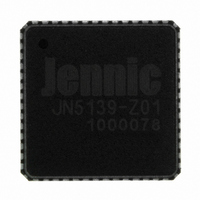
JN5139-Z01-V NXP Semiconductors, JN5139-Z01-V Datasheet - Page 75

JN5139-Z01-V
Manufacturer Part Number
JN5139-Z01-V
Description
IC MCU ZIGBEE 32BIT 2.4G 56QFN
Manufacturer
NXP Semiconductors
Series
JN5139-Z01Rxr
Specifications of JN5139-Z01-V
Frequency
2.4GHz
Modulation Or Protocol
802.15.4 Zigbee
Applications
General Purpose
Power - Output
3dBm
Sensitivity
-97dBm
Voltage - Supply
2.2 V ~ 3.6 V
Current - Receiving
34mA
Current - Transmitting
34mA
Data Interface
PCB, Surface Mount
Memory Size
96kB RAM, 192kB ROM
Antenna Connector
PCB, Surface Mount
Operating Temperature
-40°C ~ 85°C
Package / Case
56-QFN
Lead Free Status / RoHS Status
Lead free / RoHS Compliant
Data Rate - Maximum
-
Other names
616-1034-2
935293943515
JN5139-Z01-AI
JN5139-Z01-V
JN5139-Z01R1-ARV
JN5139-Z01R1V
935293943515
JN5139-Z01-AI
JN5139-Z01-V
JN5139-Z01R1-ARV
JN5139-Z01R1V
B.1.2 Crystal Load Capacitance
The crystal load capacitance is the total capacitance seen at the crystal pins, from all sources. As the load
capacitance (CL) affects the oscillation frequency by a process known as ‘pulling’, crystal manufacturers specify the
frequency for a given load capacitance only. A typical pulling coefficient is 15ppm/pF, to put this into context the
maximum frequency error in the IEEE802.15.4 specification is +/-40ppm for the transmitted signal. Therefore, it is
important for resonance at 16MHz exactly, that the specified load capacitance is provided.
The load capacitance can be calculated using:
Total capacitance
Where
Similarly for
Hence for a 9pF load capacitance, and a tight layout the external capacitors should be 15pF
B.1.3 Crystal ESR and Required Transconductance
The resistor in the crystal equivalent circuit represents the energy lost. To maintain oscillation, power must be
supplied by the amplifier, but how much? Firstly, the Pi connected capacitors C
apply an impedance transformation to Rm, when viewed from the amplifier. This new value is given by:
The amplifier is a transconductance amplifier, which takes a voltage and produces an output current. The amplifier
together with the capacitors C1 and C2, form a circuit, which provides a negative resistance, when viewed from the
crystal. The value of which is given by:
Where
Derivations of these formulas can be easily found in textbooks.
In order to give quick and reliable oscillator start-up, a common rule of thumb is to set the amplifier negative
resistance to be a minimum of 4 times the effective crystal resistance. This gives
© NXP Laboratories UK 2010
C
C
C
ω
g
m
1
1
1
is the frequency in rad/s
P
in
C
is the transconductance
is the capacitor component
is the PCB parasitic capacitance. With the recommended layout this is about 1.6pF
T
is the on-chip parasitic capacitance and is about 1.4pF typically.
2
C
T
1
×
R
C
NEG
g
C
R
T
ˆ
m
T
m
2
CL
1
JN-DS-JN5139 1v9
×
=
=
=
ω
C
=
C
R
1
2
T
+
m
C
1
C
⎛
⎜
⎜
⎝
C
×
C
T
≥
T
1
1
1
P
C
×
+
S
C
4
g
+
+
C
C
T
R
m
L
C
C
T
2
T
m
1
2
2
×
L
in
⎛
⎜
⎜
⎝
⎞
⎟
⎟
⎠
C
ω
2
S
C
2
+
L
C
L
1
and C
⎞
⎟
⎟
⎠
2
2
with C
S
from the crystal,
75


