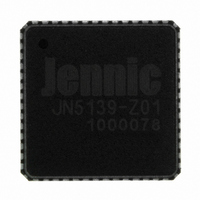
JN5139-Z01-V NXP Semiconductors, JN5139-Z01-V Datasheet - Page 33

JN5139-Z01-V
Manufacturer Part Number
JN5139-Z01-V
Description
IC MCU ZIGBEE 32BIT 2.4G 56QFN
Manufacturer
NXP Semiconductors
Series
JN5139-Z01Rxr
Specifications of JN5139-Z01-V
Frequency
2.4GHz
Modulation Or Protocol
802.15.4 Zigbee
Applications
General Purpose
Power - Output
3dBm
Sensitivity
-97dBm
Voltage - Supply
2.2 V ~ 3.6 V
Current - Receiving
34mA
Current - Transmitting
34mA
Data Interface
PCB, Surface Mount
Memory Size
96kB RAM, 192kB ROM
Antenna Connector
PCB, Surface Mount
Operating Temperature
-40°C ~ 85°C
Package / Case
56-QFN
Lead Free Status / RoHS Status
Lead free / RoHS Compliant
Data Rate - Maximum
-
Other names
616-1034-2
935293943515
JN5139-Z01-AI
JN5139-Z01-V
JN5139-Z01R1-ARV
JN5139-Z01R1V
935293943515
JN5139-Z01-AI
JN5139-Z01-V
JN5139-Z01R1-ARV
JN5139-Z01R1V
A transaction commences with the SPI bus being set to the correct configuration, and then the slave device is
selected. Upon commencement of transmission (8, 16 or 32 bits) data is placed in the FIFO data buffer and clocked
out, at the same time generating the corresponding SPICLK transitions. Since the transfer is full-duplex, the same
number of data bits is being received from the slave as it transmits. The data that is received during this transmission
can be read 8, 16 or 32 bits. If the master simply needs to provide a number of SPICLK transitions to allow data to
be sent from a slave, it should perform transmit using dummy data. An interrupt can be generated when the
transaction has completed or alternatively the interface can be polled.
If a slave device wishes to signal the JN5139 indicating that it has data to provide, it may be connected to one of the
DIO pins that can be enabled as an interrupt.
© NXP Laboratories UK 2010
JN-DS-JN5139 1v9
33


