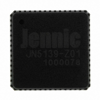
JN5139-Z01-V NXP Semiconductors, JN5139-Z01-V Datasheet - Page 30

JN5139-Z01-V
Manufacturer Part Number
JN5139-Z01-V
Description
IC MCU ZIGBEE 32BIT 2.4G 56QFN
Manufacturer
NXP Semiconductors
Series
JN5139-Z01Rxr
Specifications of JN5139-Z01-V
Frequency
2.4GHz
Modulation Or Protocol
802.15.4 Zigbee
Applications
General Purpose
Power - Output
3dBm
Sensitivity
-97dBm
Voltage - Supply
2.2 V ~ 3.6 V
Current - Receiving
34mA
Current - Transmitting
34mA
Data Interface
PCB, Surface Mount
Memory Size
96kB RAM, 192kB ROM
Antenna Connector
PCB, Surface Mount
Operating Temperature
-40°C ~ 85°C
Package / Case
56-QFN
Lead Free Status / RoHS Status
Lead free / RoHS Compliant
Data Rate - Maximum
-
Other names
616-1034-2
935293943515
JN5139-Z01-AI
JN5139-Z01-V
JN5139-Z01R1-ARV
JN5139-Z01R1V
935293943515
JN5139-Z01-AI
JN5139-Z01-V
JN5139-Z01R1-ARV
JN5139-Z01R1V
Throughout a sleep cycle the direction of the DIO, and the state of the outputs, is held. This is based on the resultant
of the GPIO Data/ Direction registers and the effect of any enabled peripherals at the point of entering sleep.
Following a wake-up these directions and output values are maintained under control of the GPIO data / direction
registers. Any peripherals enabled before the sleep cycle are not automatically re-enabled, this must be done through
software after the wake-up.
For example, if DIO0 is configured to be SPISEL1 then it becomes an output. The output value is controlled by the
SPI functional block. If the device then enters a sleep cycle, the DIO will remain an output and hold the value being
output when entering sleep. After wake-up the DIO will still be an output with the same value but controlled from the
GPIO Data/Direction registers. It can be altered with the software functions that adjust the DIO, or the application may
re-configure it to be SPISEL1.
Unused DIO pins are recommended to be set as inputs with the pull-up enabled.
30
JN-DS-JN5139 1v9
© NXP Laboratories UK 2010


