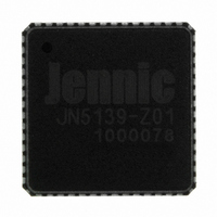
JN5139-Z01-V NXP Semiconductors, JN5139-Z01-V Datasheet - Page 19

JN5139-Z01-V
Manufacturer Part Number
JN5139-Z01-V
Description
IC MCU ZIGBEE 32BIT 2.4G 56QFN
Manufacturer
NXP Semiconductors
Series
JN5139-Z01Rxr
Specifications of JN5139-Z01-V
Frequency
2.4GHz
Modulation Or Protocol
802.15.4 Zigbee
Applications
General Purpose
Power - Output
3dBm
Sensitivity
-97dBm
Voltage - Supply
2.2 V ~ 3.6 V
Current - Receiving
34mA
Current - Transmitting
34mA
Data Interface
PCB, Surface Mount
Memory Size
96kB RAM, 192kB ROM
Antenna Connector
PCB, Surface Mount
Operating Temperature
-40°C ~ 85°C
Package / Case
56-QFN
Lead Free Status / RoHS Status
Lead free / RoHS Compliant
Data Rate - Maximum
-
Other names
616-1034-2
935293943515
JN5139-Z01-AI
JN5139-Z01-V
JN5139-Z01R1-ARV
JN5139-Z01R1V
935293943515
JN5139-Z01-AI
JN5139-Z01-V
JN5139-Z01R1-ARV
JN5139-Z01R1V
6 Reset
A system reset initialises the device to a predefined state and forces the CPU to start program execution from the
reset vector. The reset process that the JN5139 goes through is as follows.
When power is applied, the internal 32kHz oscillator starts up and stabilises, which takes approximately 100μsec. At
this point, the 16MHz crystal oscillator is enabled and power is applied to the processor and digital logic. The logic
blocks are held in reset until the 16MHz crystal oscillator stabilises, which typically takes 2.75ms.
Once the oscillator is up and running the internal reset is removed from the CPU and peripheral logic and the CPU
starts to run code beginning at the reset vector, consisting of initialisation code and the resident Boot Loader
(described in JN-AN-1003 Boot Loader Operation [2]).
Section 17.3.1 provides detailed electrical data and timing.
The JN5139 has three sources of reset:
When reset is low, the digital logic and RAM are not powered and therefore anything stored in the RAM after reset is
released cannot be guaranteed to still be valid.
6.1 Internal Power-on Reset
For the majority of applications the internal power-on reset is capable of generating the required reset signal. When
power is applied to the device, the power-on reset circuit monitors the rise of the VDD supply. When VDD reaches
the specified threshold, the reset signal is generated and can be observed as a rising edge on the RESETN pin. This
signal is held internally until the power supply and oscillator stabilisation time has elapsed, at which point the internal
reset signal is then removed and the CPU is allowed to run.
The external resistor and capacitor provides a simple reset operation when connected to the RESETN pin, as shown
in Figure 11. This can be used to extend the reset length and help in systems with noisy reset push-buttons.
© NXP Laboratories UK 2010
•
•
•
Internal Power-on Reset
External Reset
Software Reset
Note: When the device exits a reset condition, device operating
parameters (voltage, frequency, temperature, etc.) must be met to ensure
operation. If these conditions are not met, then the device must be held in
reset until the operating conditions are met. (See section 17.3.1)
Internal RESET
RESETN Pin
VDD
Figure 10: Internal Power-on Reset
JN-DS-JN5139 1v9
19


