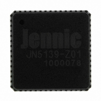
JN5139-Z01-V NXP Semiconductors, JN5139-Z01-V Datasheet - Page 39

JN5139-Z01-V
Manufacturer Part Number
JN5139-Z01-V
Description
IC MCU ZIGBEE 32BIT 2.4G 56QFN
Manufacturer
NXP Semiconductors
Series
JN5139-Z01Rxr
Specifications of JN5139-Z01-V
Frequency
2.4GHz
Modulation Or Protocol
802.15.4 Zigbee
Applications
General Purpose
Power - Output
3dBm
Sensitivity
-97dBm
Voltage - Supply
2.2 V ~ 3.6 V
Current - Receiving
34mA
Current - Transmitting
34mA
Data Interface
PCB, Surface Mount
Memory Size
96kB RAM, 192kB ROM
Antenna Connector
PCB, Surface Mount
Operating Temperature
-40°C ~ 85°C
Package / Case
56-QFN
Lead Free Status / RoHS Status
Lead free / RoHS Compliant
Data Rate - Maximum
-
Other names
616-1034-2
935293943515
JN5139-Z01-AI
JN5139-Z01-V
JN5139-Z01R1-ARV
JN5139-Z01R1V
935293943515
JN5139-Z01-AI
JN5139-Z01-V
JN5139-Z01R1-ARV
JN5139-Z01R1V
12.1.5 Timer / Counter Application
Figure 31 shows an application of the JN5139 timers to provide closed loop speed control. Timer 0 is configured in
PWM mode to provide a variable mark-space ratio switching waveform to the gate of the NFET. This in turn controls
the power in the DC motor.
Timer 1 is configured to count the rising edge events on the clk/gate pin over a constant period. This converts the
tacho pulse stream output into a count proportional to the motor speed. This value is then used by the application
software executing the control algorithm.
© NXP Laboratories UK 2010
Timer 0
Timer 1
JN5139
Figure 31: Closed Loop PWM Speed Control Using JN5139 Timers
51
48
50
52
53
54
CLK/GATE
CAPTURE
CLK/GATE
CAPTURE
PWM
PWM
JN-DS-JN5139 1v9
1N4007
M
IRF521
1 pulse/rev
Tacho
+12V
39


