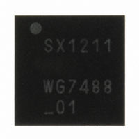
SX1211I084TRT Semtech, SX1211I084TRT Datasheet - Page 33

SX1211I084TRT
Manufacturer Part Number
SX1211I084TRT
Description
IC SNGL-CHIP TXRX 32-TQFN
Manufacturer
Semtech
Specifications of SX1211I084TRT
Frequency
860 ~ 960MHz
Data Rate - Maximum
200kbps
Modulation Or Protocol
FSK, OOK
Applications
AMR, ISM, Security and Access
Power - Output
12.5dBm
Sensitivity
-113dBm
Voltage - Supply
2.1 V ~ 3.6 V
Current - Receiving
3mA
Current - Transmitting
25mA
Data Interface
PCB, Surface Mount
Antenna Connector
PCB, Surface Mount
Operating Temperature
-40°C ~ 85°C
Package / Case
32-TQFN
Operating Temperature (min)
-40C
Operating Temperature (max)
85C
Operating Temperature Classification
Industrial
Modulation Type
FSK/OOK
Package Type
TQFN EP
Operating Supply Voltage (min)
2.1V
Operating Supply Voltage (typ)
2.5/3.3V
Operating Supply Voltage (max)
3.6V
Lead Free Status / RoHS Status
Lead free / RoHS Compliant
Memory Size
-
Lead Free Status / Rohs Status
Compliant
Other names
SX1211I084TRT
Available stocks
Company
Part Number
Manufacturer
Quantity
Price
Company:
Part Number:
SX1211I084TRT
Manufacturer:
HITTITE
Quantity:
560
4. Operating Modes
This section summarizes the settings for each operating mode of the SX1211, and explains the functionality
available and the timing requirements for switching between modes.
Table 12: Operating Modes
Table 13 describes the state of the digital IOs in each of the above described modes of operation, regardless of the
data operating mode (Continuous, Buffered, or Packet).
Table 13: Pin Configuration vs. Chip Mode
Notes:
(1): High-Z if Continuous mode is activated, else Output
(2): Output if PLL_lock_en = 1, else High-Z
(3): Valid logic states must be applied to inputs at all times to avoid unwanted leakage currents
Rev 7 – Sept 2
ADVANCED COMMUNICATIONS & SENSING
Mode
Sleep
Standby
FS
Receive
Transmit
……….Mode
NSS_CONFIG
NSS_DATA
MISO
MOSI
SCK
IRQ_0
IRQ_1
DATA
CLKOUT
PLL_LOCK
4.1. Modes of Operation
4.2. Digital Pin Configuration vs. Chip Mode
Pin
Chip
nd
, 2008
MCParam_Chip_mode
Sleep
mode
Input
Input
Input
Input
Input
High-Z
High-Z
Input
High-Z
High-Z
000
001
010
011
100
Standby
mode
Input
Input
Input
Input
Input
Output (1)
Output (1)
Input
Output
Output (2)
Active blocks
SPI, POR
SPI, POR, Top regulator, digital regulator, XO, CLKOUT (if activated through
OSCParam_Clkout)
Same + VCO regulator, all PLL and LO generation blocks
Same as FS mode + LNA, first mixer, IF amplifier, second mixer set, channel
filters, baseband amplifiers and limiters, RSSI, OOK or FSK demodulator,
BitSync and all digital features if enabled
Same as FS mode + DDS, Interpolation filters, all up-conversion mixers, PA
driver, PA and external VR_PA pin output for PA choke.
FS mode
Input
Input
Input
Input
Input
Output (1)
Output (1)
Input
Output
Output (2)
Page 33 of 92
Receive
mode
Input
Input
Input
Input
Input
Output
Output
Output
Output
Output (2)
Transmit
mode
Input
Input
Input
Input
Input
Output
Output
Input
Output
Output (2)
Comment
NSS_CONFIG has the priority over
NSS_DATA
Output only if NSS_CONFIG or
NSSDATA=’0’
www.semtech.com
SX1211


