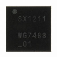
SX1211I084TRT Semtech, SX1211I084TRT Datasheet - Page 34

SX1211I084TRT
Manufacturer Part Number
SX1211I084TRT
Description
IC SNGL-CHIP TXRX 32-TQFN
Manufacturer
Semtech
Specifications of SX1211I084TRT
Frequency
860 ~ 960MHz
Data Rate - Maximum
200kbps
Modulation Or Protocol
FSK, OOK
Applications
AMR, ISM, Security and Access
Power - Output
12.5dBm
Sensitivity
-113dBm
Voltage - Supply
2.1 V ~ 3.6 V
Current - Receiving
3mA
Current - Transmitting
25mA
Data Interface
PCB, Surface Mount
Antenna Connector
PCB, Surface Mount
Operating Temperature
-40°C ~ 85°C
Package / Case
32-TQFN
Operating Temperature (min)
-40C
Operating Temperature (max)
85C
Operating Temperature Classification
Industrial
Modulation Type
FSK/OOK
Package Type
TQFN EP
Operating Supply Voltage (min)
2.1V
Operating Supply Voltage (typ)
2.5/3.3V
Operating Supply Voltage (max)
3.6V
Lead Free Status / RoHS Status
Lead free / RoHS Compliant
Memory Size
-
Lead Free Status / Rohs Status
Compliant
Other names
SX1211I084TRT
Available stocks
Company
Part Number
Manufacturer
Quantity
Price
Company:
Part Number:
SX1211I084TRT
Manufacturer:
HITTITE
Quantity:
560
5. Data Processing
Figure 25, illustrates the SX1211 data processing circuit. Its role is to interface the data to/from the
modulator/demodulator and the uC access points (SPI, IRQ and DATA pins). It also controls all the configuration
registers.
The circuit contains several control blocks which are described in the following paragraphs.
The SX1211 implements several data operation modes, each with their own data path through the data processing
section. Depending on the data operation mode selected, some control blocks are active whilst others remain
disabled.
The SX1211 has three different data operation modes selectable by the user:
Rev 7 – Sept 2
ADVANCED COMMUNICATIONS & SENSING
5.1. Overview
Continuous mode: each bit transmitted or received is accessed in real time at the DATA pin. This mode may be
used if adequate external signal processing is available.
Buffered mode: each byte transmitted or received is stored in a FIFO and accessed via the SPI bus. uC
processing overhead is hence significantly reduced compared to Continuous mode operation. The packet
length is unlimited.
Packet mode (recommended): user only provides/retrieves payload bytes to/from the FIFO. The packet is
automatically built with preamble, Sync word, and optional CRC, DC free encoding and the reverse operation is
performed in reception. The uC processing overhead is hence reduced further compared to Buffered mode.
The maximum payload length is limited to the maximum FIFO limit of 64 bytes
Data
5.1.1. Block Diagram
5.1.2. Data Operation Modes
nd
Tx/Rx
, 2008
Tx
Rx
SYNC
RECOG.
Figure 25: SX1211’s Data Processing Conceptual View
PACKET
HANDLER
SX1211
CONTROL
Page 34 of 92
FIFO
(+SR)
CONFIG
DATA
SPI
www.semtech.com
SX1211
MISO
SCK
MOSI
NSS_DATA
IRQ_1
DATA
IRQ_0


