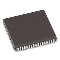
XR16C854IJ-F Exar Corporation, XR16C854IJ-F Datasheet - Page 28

XR16C854IJ-F
Manufacturer Part Number
XR16C854IJ-F
Description
IC UART FIFO 128B QUAD 68PLCC
Manufacturer
Exar Corporation
Datasheet
1.XR16C854IV-F.pdf
(54 pages)
Specifications of XR16C854IJ-F
Features
*
Number Of Channels
4, QUART
Fifo's
128 Byte
Protocol
RS232, RS485
Voltage - Supply
2.97 V ~ 5.5 V
With Auto Flow Control
Yes
With Irda Encoder/decoder
Yes
With False Start Bit Detection
Yes
With Modem Control
Yes
With Cmos
Yes
Mounting Type
Surface Mount
Package / Case
68-LCC (J-Lead)
No. Of Channels
4
Data Rate
2Mbps
Supply Voltage Range
2.97V To 5.5V
Operating Temperature Range
-40°C To +85°C
Digital Ic Case Style
PLCC
No. Of Pins
68
Termination Type
SMD
Uart Features
Tx/Rx FIFO Counters
Rohs Compliant
Yes
Lead Free Status / RoHS Status
Lead free / RoHS Compliant
Available stocks
Company
Part Number
Manufacturer
Quantity
Price
Company:
Part Number:
XR16C854IJ-F
Manufacturer:
EXAR
Quantity:
4
Company:
Part Number:
XR16C854IJ-F
Manufacturer:
Exar Corporation
Quantity:
10 000
XR16C854/854D
2.97V TO 5.5V QUAD UART WITH 128-BYTE FIFO
]
ISR[0]: Interrupt Status
•
•
ISR[3:1]: Interrupt Status
These bits indicate the source for a pending interrupt at interrupt priority levels (See Interrupt Source
Table
ISR[5:4]: Interrupt Status
These bits are enabled when EFR bit-4 is set to a logic 1. ISR bit-4 indicates that the receiver detected a data
match of the Xoff character(s). Note that once set to a logic 1, the ISR bit-4 will stay a logic 1 until a Xon
character is received. ISR bit-5 indicates that CTS# or RTS# has changed state.
ISR[7:6]: FIFO Enable Status
These bits are set to a logic 0 when the FIFOs are disabled. They are set to a logic 1 when the FIFOs are
enabled.
This register is used to enable the FIFOs, clear the FIFOs, set the transmit/receive FIFO trigger levels, and
select the DMA mode. The DMA and FIFO modes are defined as follows:
FCR[0]: TX and RX FIFO Enable
•
•
FCR[1]: RX FIFO Reset
This bit is only active when FCR bit-0 is a ‘1’.
•
•
4.5
P
Logic 0 = An interrupt is pending and the ISR contents may be used as a pointer to the appropriate interrupt
service routine.
Logic 1 = No interrupt pending (default condition).
Logic 0 = Disable the transmit and receive FIFO (default).
Logic 1 = Enable the transmit and receive FIFOs. This bit must be set to logic 1 when other FCR bits are
written or they will not be programmed.
Logic 0 = No receive FIFO reset (default)
Logic 1 = Reset the receive FIFO pointers and FIFO level counter logic (the receive shift register is not
cleared or altered). This bit will return to a logic 0 after resetting the FIFO.
L
RIORITY
EVEL
1
2
3
4
5
6
7
-
10).
FIFO Control Register (FCR) - Write-Only
B
IT
0
0
0
0
0
0
1
0
-5
B
IT
0
0
0
0
0
1
0
0
-4
ISR R
B
T
EGISTER
IT
0
1
0
0
0
0
0
0
ABLE
-3
10: I
B
S
IT
TATUS
1
1
1
0
0
0
0
0
-2
NTERRUPT
B
B
ITS
IT
1
0
0
1
0
0
0
0
-1
S
OURCE AND
28
B
IT
0
0
0
0
0
0
0
1
-0
LSR (Receiver Line Status Register)
RXRDY (Receive Data Time-out)
RXRDY (Received Data Ready)
TXRDY (Transmit Ready)
MSR (Modem Status Register)
RXRDY (Received Xoff or Special character)
CTS#, RTS# change of state
None (default)
P
RIORITY
L
EVEL
S
OURCE OF INTERRUPT
xr
REV. 3.0.1


