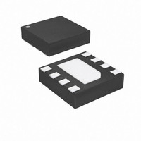
ATTINY5-MAH Atmel, ATTINY5-MAH Datasheet - Page 49

ATTINY5-MAH
Manufacturer Part Number
ATTINY5-MAH
Description
IC MCU AVR 512B FLASH 8UDFN
Manufacturer
Atmel
Series
AVR® ATtinyr
Specifications of ATTINY5-MAH
Core Processor
AVR
Core Size
8-Bit
Speed
12MHz
Peripherals
POR, PWM, WDT
Number Of I /o
4
Program Memory Size
512B (256 x 16)
Program Memory Type
FLASH
Ram Size
32 x 8
Voltage - Supply (vcc/vdd)
1.8 V ~ 5.5 V
Data Converters
A/D 4x8b
Oscillator Type
Internal
Operating Temperature
-40°C ~ 85°C
Package / Case
8-UFDFN Exposed Pad
Core
AVR8
Lead Free Status / RoHS Status
Lead free / RoHS Compliant
Eeprom Size
-
Connectivity
-
Lead Free Status / Rohs Status
Details
- Current page: 49 of 169
- Download datasheet (5Mb)
10.3.1
8127D–AVR–02/10
Alternate Functions of Port B
The Port B pins with alternate function are shown in
Table 10-3.
• Port B, Bit 0 – ADC0/AIN0/OC0A/PCINT0/TPIDATA
• Port B, Bit 1 – ADC1/AIN1/CLKI/ICP0/OC0B/PCINT1/TPICLK
• ADC0: Analog to Digital Converter, Channel 0
• AIN0: Analog Comparator Positive Input. Configure the port pin as input with the internal pull-
• OC0A, Output Compare Match output: The PB0 pin can serve as an external output for the
• PCINT0: Pin Change Interrupt source 0. The PB0 pin can serve as an external interrupt
• TPIDATA: Serial Programming Data.
• ADC1: Analog to Digital Converter, Channel 1
• AIN1: Analog Comparator Negative Input. Configure the port pin as input with the internal
• CLKI: External Clock.
• ICP0: Input Capture Pin. The PB1 pin can act as an Input Capture pin for Timer/Counter0.
up switched off to avoid the digital port function from interfering with the function of the
Analog Comparator.
Timer/Counter0 Compare Match A. The pin has to be configured as an output (DDB0 set
(one)) to serve this function. This is also the output pin for the PWM mode timer function.
source for pin change interrupt 0.
pull-up switched off to avoid the digital port function from interfering with the function of the
Analog Comparator.
Port Pin
PB0
PB1
PB2
PB3
Port B Pins Alternate Functions
Alternate Function
ADC0:
AIN0:
OC0A: Timer/Counter0 Compare Match A Output
PCINT0: Pin Change Interrupt 0, Source 0
TPIDATA:Serial Programming Data
ADC1:
AIN1:
CLKI:
ICP0:
OC0B: Timer/Counter0 Compare Match B Output
PCINT1:Pin Change Interrupt 0, Source 1
TPICLK: Serial Programming Clock
ADC2:
CLKO: System Clock Output
INT0:
PCINT2: Pin Change Interrupt 0, Source 2
T0:
ADC3:
PCINT3: Pin Change Interrupt 0, Source 3
RESET: Reset Pin
ADC Input Channel 0
Analog Comparator, Positive Input
ADC Input Channel 1
Analog Comparator, Negative Input
External Clock
Timer/Counter0 Input Capture Input
ADC Input Channel 2
External Interrupt 0 Source
Timer/Counter0 Clock Source
ADC Input Channel 3
(ATtiny5/10, only)
(ATtiny5/10, only)
Table 10-3 on page
ATtiny4/5/9/10
49.
49
Related parts for ATTINY5-MAH
Image
Part Number
Description
Manufacturer
Datasheet
Request
R

Part Number:
Description:
Manufacturer:
Atmel Corporation
Datasheet:

Part Number:
Description:
IC MCU AVR 512B FLASH SOT-23-6
Manufacturer:
Atmel
Datasheet:

Part Number:
Description:
IC MCU AVR 512B FLASH 8UDFN
Manufacturer:
Atmel
Datasheet:

Part Number:
Description:
IC MCU AVR 512B FLASH SOT-23-6
Manufacturer:
Atmel
Datasheet:

Part Number:
Description:
IC, MCU, 8BIT, 2K FLASH, 20SOIC
Manufacturer:
Atmel
Datasheet:

Part Number:
Description:
IC, MCU, 8BIT, 2K FLASH, 20PDIP
Manufacturer:
Atmel
Datasheet:

Part Number:
Description:
IC, MCU, 8BIT, 8K FLASH, 20PDIP
Manufacturer:
Atmel
Datasheet:

Part Number:
Description:
IC, MCU, 8BIT, 8K FLASH, 20SOIC
Manufacturer:
Atmel
Datasheet:

Part Number:
Description:
DEV KIT FOR AVR/AVR32
Manufacturer:
Atmel
Datasheet:

Part Number:
Description:
INTERVAL AND WIPE/WASH WIPER CONTROL IC WITH DELAY
Manufacturer:
ATMEL Corporation
Datasheet:

Part Number:
Description:
Low-Voltage Voice-Switched IC for Hands-Free Operation
Manufacturer:
ATMEL Corporation
Datasheet:

Part Number:
Description:
MONOLITHIC INTEGRATED FEATUREPHONE CIRCUIT
Manufacturer:
ATMEL Corporation
Datasheet:

Part Number:
Description:
AM-FM Receiver IC U4255BM-M
Manufacturer:
ATMEL Corporation
Datasheet:

Part Number:
Description:
Monolithic Integrated Feature Phone Circuit
Manufacturer:
ATMEL Corporation
Datasheet:


