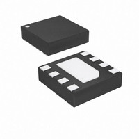
ATTINY5-MAH Atmel, ATTINY5-MAH Datasheet - Page 67

ATTINY5-MAH
Manufacturer Part Number
ATTINY5-MAH
Description
IC MCU AVR 512B FLASH 8UDFN
Manufacturer
Atmel
Series
AVR® ATtinyr
Specifications of ATTINY5-MAH
Core Processor
AVR
Core Size
8-Bit
Speed
12MHz
Peripherals
POR, PWM, WDT
Number Of I /o
4
Program Memory Size
512B (256 x 16)
Program Memory Type
FLASH
Ram Size
32 x 8
Voltage - Supply (vcc/vdd)
1.8 V ~ 5.5 V
Data Converters
A/D 4x8b
Oscillator Type
Internal
Operating Temperature
-40°C ~ 85°C
Package / Case
8-UFDFN Exposed Pad
Core
AVR8
Lead Free Status / RoHS Status
Lead free / RoHS Compliant
Eeprom Size
-
Connectivity
-
Lead Free Status / Rohs Status
Details
- Current page: 67 of 169
- Download datasheet (5Mb)
8127D–AVR–02/10
operation. However, due to the symmetric feature of the dual-slope PWM modes, these modes
are preferred for motor control applications.
The PWM resolution for the phase correct PWM mode can be fixed to 8-, 9-, or 10-bit, or defined
by either ICR0 or OCR0A. The minimum resolution allowed is 2-bit (ICR0 or OCR0A set to
0x0003), and the maximum resolution is 16-bit (ICR0 or OCR0A set to MAX). The PWM resolu-
tion in bits can be calculated by using the following equation:
In phase correct PWM mode the counter is incremented until the counter value matches either
one of the fixed values 0x00FF, 0x01FF, or 0x03FF (WGM03:0 = 1, 2, or 3), the value in ICR0
(WGM03:0 = 10), or the value in OCR0A (WGM03:0 = 11). The counter has then reached the
TOP and changes the count direction. The TCNT0 value will be equal to TOP for one timer clock
cycle. The timing diagram for the phase correct PWM mode is shown on
67. The figure shows phase correct PWM mode when OCR0A or ICR0 is used to define TOP.
The TCNT0 value is in the timing diagram shown as a histogram for illustrating the dual-slope
operation. The diagram includes non-inverted and inverted PWM outputs. The small horizontal
line marks on the TCNT0 slopes represent compare matches between OCR0x and TCNT0. The
OC0x interrupt flag will be set when a compare match occurs.
Figure 11-10. Phase Correct PWM Mode, Timing Diagram
The Timer/Counter Overflow Flag (TOV0) is set each time the counter reaches BOTTOM. When
either OCR0A or ICR0 is used for defining the TOP value, the OC0A or ICF0 flag is set accord-
ingly at the same timer clock cycle as the OCR0x Registers are updated with the double buffer
value (at TOP). The interrupt flags can be used to generate an interrupt each time the counter
reaches the TOP or BOTTOM value.
When changing the TOP value the program must ensure that the new TOP value is higher or
equal to the value of all of the Compare Registers. If the TOP value is lower than any of the
TCNTn
OCnx
OCnx
Period
1
R
PCPWM
2
=
log
---------------------------------- -
(
log
TOP
3
2 ( )
+
1
)
ATtiny4/5/9/10
4
Figure 11-10 on page
OCRnx/TOP Update and
OCnA Interrupt Flag Set
or ICFn Interrupt Flag Set
(Interrupt on TOP)
TOVn Interrupt Flag Set
(Interrupt on Bottom)
(COMnx1:0 = 2)
(COMnx1:0 = 3)
67
Related parts for ATTINY5-MAH
Image
Part Number
Description
Manufacturer
Datasheet
Request
R

Part Number:
Description:
Manufacturer:
Atmel Corporation
Datasheet:

Part Number:
Description:
IC MCU AVR 512B FLASH SOT-23-6
Manufacturer:
Atmel
Datasheet:

Part Number:
Description:
IC MCU AVR 512B FLASH 8UDFN
Manufacturer:
Atmel
Datasheet:

Part Number:
Description:
IC MCU AVR 512B FLASH SOT-23-6
Manufacturer:
Atmel
Datasheet:

Part Number:
Description:
IC, MCU, 8BIT, 2K FLASH, 20SOIC
Manufacturer:
Atmel
Datasheet:

Part Number:
Description:
IC, MCU, 8BIT, 2K FLASH, 20PDIP
Manufacturer:
Atmel
Datasheet:

Part Number:
Description:
IC, MCU, 8BIT, 8K FLASH, 20PDIP
Manufacturer:
Atmel
Datasheet:

Part Number:
Description:
IC, MCU, 8BIT, 8K FLASH, 20SOIC
Manufacturer:
Atmel
Datasheet:

Part Number:
Description:
DEV KIT FOR AVR/AVR32
Manufacturer:
Atmel
Datasheet:

Part Number:
Description:
INTERVAL AND WIPE/WASH WIPER CONTROL IC WITH DELAY
Manufacturer:
ATMEL Corporation
Datasheet:

Part Number:
Description:
Low-Voltage Voice-Switched IC for Hands-Free Operation
Manufacturer:
ATMEL Corporation
Datasheet:

Part Number:
Description:
MONOLITHIC INTEGRATED FEATUREPHONE CIRCUIT
Manufacturer:
ATMEL Corporation
Datasheet:

Part Number:
Description:
AM-FM Receiver IC U4255BM-M
Manufacturer:
ATMEL Corporation
Datasheet:

Part Number:
Description:
Monolithic Integrated Feature Phone Circuit
Manufacturer:
ATMEL Corporation
Datasheet:


