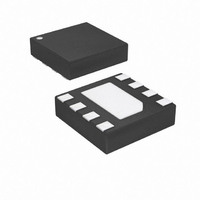
ATTINY5-MAH Atmel, ATTINY5-MAH Datasheet - Page 60

ATTINY5-MAH
Manufacturer Part Number
ATTINY5-MAH
Description
IC MCU AVR 512B FLASH 8UDFN
Manufacturer
Atmel
Series
AVR® ATtinyr
Specifications of ATTINY5-MAH
Core Processor
AVR
Core Size
8-Bit
Speed
12MHz
Peripherals
POR, PWM, WDT
Number Of I /o
4
Program Memory Size
512B (256 x 16)
Program Memory Type
FLASH
Ram Size
32 x 8
Voltage - Supply (vcc/vdd)
1.8 V ~ 5.5 V
Data Converters
A/D 4x8b
Oscillator Type
Internal
Operating Temperature
-40°C ~ 85°C
Package / Case
8-UFDFN Exposed Pad
Core
AVR8
Lead Free Status / RoHS Status
Lead free / RoHS Compliant
Eeprom Size
-
Connectivity
-
Lead Free Status / Rohs Status
Details
- Current page: 60 of 169
- Download datasheet (5Mb)
11.6
60
Output Compare Units
ATtiny4/5/9/10
cleared by software (writing a logical one to the I/O bit location). For measuring frequency only,
the clearing of the ICF0 flag is not required (if an interrupt handler is used).
The 16-bit comparator continuously compares TCNT0 with the Output Compare Register
(OCR0x). If TCNT equals OCR0x the comparator signals a match. A match will set the Output
Compare Flag (OCF0x) at the next timer clock cycle. If enabled (OCIE0x = 1), the Output Com-
pare Flag generates an Output Compare interrupt. The OCF0x flag is automatically cleared
when the interrupt is executed. Alternatively the OCF0x flag can be cleared by software by writ-
ing a logical one to its I/O bit location. The Waveform Generator uses the match signal to
generate an output according to operating mode set by the Waveform Generation mode
(WGM03:0) bits and Compare Output mode (COM0x1:0) bits. The TOP and BOTTOM signals
are used by the Waveform Generator for handling the special cases of the extreme values in
some modes of operation
A special feature of Output Compare unit A allows it to define the Timer/Counter TOP value (i.e.,
counter resolution). In addition to the counter resolution, the TOP value defines the period time
for waveforms generated by the Waveform Generator.
Figure 11-6 on page 60
register and bit names indicates the device number (n = 0 for Timer/Counter 0), and the “x” indi-
cates Output Compare unit (A/B). The elements of the block diagram that are not directly a part
of the Output Compare unit are gray shaded.
Figure 11-6. Output Compare Unit, Block Diagram
The OCR0x Register is double buffered when using any of the twelve Pulse Width Modulation
(PWM) modes. For the Normal and Clear Timer on Compare (CTC) modes of operation, the
OCRnxH Buf. (8-bit)
shows a block diagram of the Output Compare unit. The small “n” in the
OCRnxH (8-bit)
(“Modes of Operation” on page
BOTTOM
OCRnx Buffer (16-bit Register)
TEMP (8-bit)
TOP
OCRnx (16-bit Register)
OCRnxL Buf. (8-bit)
OCRnxL (8-bit)
DATA BUS
Waveform Generator
WGMn3:0
=
(16-bit Comparator )
(8-bit)
63).
COMnx1:0
TCNTnH (8-bit)
OCFnx (Int.Req.)
TCNTn (16-bit Counter)
TCNTnL (8-bit)
8127D–AVR–02/10
OCnx
Related parts for ATTINY5-MAH
Image
Part Number
Description
Manufacturer
Datasheet
Request
R

Part Number:
Description:
Manufacturer:
Atmel Corporation
Datasheet:

Part Number:
Description:
IC MCU AVR 512B FLASH SOT-23-6
Manufacturer:
Atmel
Datasheet:

Part Number:
Description:
IC MCU AVR 512B FLASH 8UDFN
Manufacturer:
Atmel
Datasheet:

Part Number:
Description:
IC MCU AVR 512B FLASH SOT-23-6
Manufacturer:
Atmel
Datasheet:

Part Number:
Description:
IC, MCU, 8BIT, 2K FLASH, 20SOIC
Manufacturer:
Atmel
Datasheet:

Part Number:
Description:
IC, MCU, 8BIT, 2K FLASH, 20PDIP
Manufacturer:
Atmel
Datasheet:

Part Number:
Description:
IC, MCU, 8BIT, 8K FLASH, 20PDIP
Manufacturer:
Atmel
Datasheet:

Part Number:
Description:
IC, MCU, 8BIT, 8K FLASH, 20SOIC
Manufacturer:
Atmel
Datasheet:

Part Number:
Description:
DEV KIT FOR AVR/AVR32
Manufacturer:
Atmel
Datasheet:

Part Number:
Description:
INTERVAL AND WIPE/WASH WIPER CONTROL IC WITH DELAY
Manufacturer:
ATMEL Corporation
Datasheet:

Part Number:
Description:
Low-Voltage Voice-Switched IC for Hands-Free Operation
Manufacturer:
ATMEL Corporation
Datasheet:

Part Number:
Description:
MONOLITHIC INTEGRATED FEATUREPHONE CIRCUIT
Manufacturer:
ATMEL Corporation
Datasheet:

Part Number:
Description:
AM-FM Receiver IC U4255BM-M
Manufacturer:
ATMEL Corporation
Datasheet:

Part Number:
Description:
Monolithic Integrated Feature Phone Circuit
Manufacturer:
ATMEL Corporation
Datasheet:


