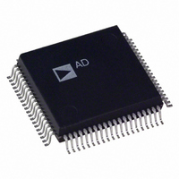
AD6620AS Analog Devices Inc, AD6620AS Datasheet - Page 37

AD6620AS
Manufacturer Part Number
AD6620AS
Description
IC DGTL RCVR SIGNAL PROC 80-PQFP
Manufacturer
Analog Devices Inc
Datasheet
1.AD6620SPCB.pdf
(44 pages)
Specifications of AD6620AS
Rohs Status
RoHS non-compliant
Interface
Parallel/Serial
Voltage - Supply
3 V ~ 3.6 V
Package / Case
80-MQFP, 80-PQFP
Mounting Type
*
Applications
-
Available stocks
Company
Part Number
Manufacturer
Quantity
Price
Part Number:
AD6620AS
Manufacturer:
ADI/亚德诺
Quantity:
20 000
Company:
Part Number:
AD6620ASZ
Manufacturer:
Analog Devices Inc
Quantity:
10 000
Company:
Part Number:
AD6620ASZ-REEL
Manufacturer:
Analog Devices Inc
Quantity:
10 000
Master AD6620, the SDFE signal will be driven high by the
same SCLK rising edge that this bit is clocked out on. On the
falling edge of this SCLK cycle, the Cascaded AD6620 will
sample its SDFS signal, which is hardwired to the SDFE of the
Master. On the very next SCLK edge, A channel: I data of the
Cascaded AD6620 will start shifting out of the port. There will
be no rest between the time-slots of the master and slave.
WL[1:0]
WL defines the Word Length of the serial data stream. The
possible options are 00–16 bit words, 01–24 bit words, 10–32 bit
words and 11–Undefined. This setting controls the width of all
serial words. All words are shifted MSB first and are left justified,
i.e., the first n-bits are valid and any padding that is needed
to fill the word length is added at the end. When the serial word
length is 24 or 32 bits, the I and Q output data is presented with
23-bit resolution.
Serial Word Length
16-Bit
24-Bit
32-Bit
Disallowed
AD
Append Data signal. In Single Channel Real Mode, when AD is
low the serial data stream consists only of A channel: I and Q
data. If the AD6620 is in Diversity Channel Real Mode, the
serial frame is four words long and consists of both A and B
channel complex data. When the AD signal is high, an extra
serial word is appended to the Serial Frame. This word consists
of any data that is read from the AD6620 internal registers via
the Serial Port. If a Read has not occurred, the data in this word
is zero. The addition of this word allows a Serial System to be
designed so that any AD6620 can have data read at any time
without changing the fixed timing of the serial port.
If the serial transfer includes a register read, the register data is
appended to the serial frame regardless of the state of the AD pin.
SDIV[3:0]
When the AD6620 is used as a Serial Bus Master the chip gen-
erates a serial clock by dividing down the CLK signal. The
divider ratio is set by the serial division word, SDIV. SDIV is
interpreted as a 4-bit unsigned integer and determines the fre-
quency of the serial clock when the SBM pin is pulled high.
When the AD6620 is in Serial Cascade Mode these bits are
ignored. The following equations express the Serial Clock Fre-
quency as a function of the CLK signal and the SDIV nibble.
Serial Port Guidelines
The serial clock, SCLK, must be run at a rate sufficient to clock
all of the serial data out of the port before new data is latched
into the internal I and Q data registers. See the Serial Output
Data Port section for more details. If the serial port is to be used
Table XVII. Setting Serial Word Length
f
SCLK
f
SCLK
=
2
=
×
f
f
CLK
CLK
SDIV
2
,
WL1
0
0
1
1
SDIV
,
SDIV
=
0
≠
0
WL0
0
1
0
1
as a means of programming the part, some extra serial bandwidth
may also be required to shift data from the internal registers of
the AD6620. There must be two or more or zero high speed
clocks between serial frames. When used as a serial bus master
SCLK can run at a maximum rate of half the processing CLK.
In serial slave mode, the serial clock can be run up to 67 MHz.
The equations below help determine what the minimum serial
clock rate must be in order to insure that data is not lost.
R
serial port: otherwise R
width consumed when data is read from the internal control
registers or memory.
JTAG BOUNDARY SCAN
The AD6620 supports a subset of IEEE Standard 1149.1
specifications. For additional details of the standard, please see
“IEEE Standard Test Access Port and Boundary-Scan
Architecture,” IEEE-1149 publication from IEEE.
The AD6620 has five pins associated with the JTAG interface.
These pins are used to access the on-chip Test Access Port
(TAP) and are listed in the table below.
The AD6620 supports four op codes as shown below. These
instructions set the mode of the JTAG interface.
The Vendor Identification Code can be accessed through the
IDCODE instruction and has the following format.
MSB
Version Part Number
0000
A BSDL file for this device is available from Analog Devices,
Inc. Contact Analog Devices, Inc. for more information.
D
= 1 if AD is asserted or if read operations are used from the
0010 0111 0111 1110 000 1110 0101
f
Pin Name
TRST
TCLK
TMS
TDI
TDO
Instruction
IDCODE
BYPASS
SAMPLE/PRELOAD
EXTEST
SCLK
M
TOT
≥
f
SAMP
=
D
M
= 0. This term accounts for the band-
Table XVIII.
Table XIX.
Table XX.
CIC
×
WL
2
Description
TAP Reset
Test Clock
TAP Mode Select
Test Data Input
Test Data Output
Manufacturing ID #
×
M
×
M
(
TOT
CIC
2
×
5
Op Code
01
11
10
00
N
×
CH
M
RCF
+
AD6620
R
D
)
LSB
Mandatory
1


