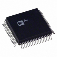
AD6620AS Analog Devices Inc, AD6620AS Datasheet - Page 41

AD6620AS
Manufacturer Part Number
AD6620AS
Description
IC DGTL RCVR SIGNAL PROC 80-PQFP
Manufacturer
Analog Devices Inc
Datasheet
1.AD6620SPCB.pdf
(44 pages)
Specifications of AD6620AS
Rohs Status
RoHS non-compliant
Interface
Parallel/Serial
Voltage - Supply
3 V ~ 3.6 V
Package / Case
80-MQFP, 80-PQFP
Mounting Type
*
Applications
-
Available stocks
Company
Part Number
Manufacturer
Quantity
Price
Part Number:
AD6620AS
Manufacturer:
ADI/亚德诺
Quantity:
20 000
Company:
Part Number:
AD6620ASZ
Manufacturer:
Analog Devices Inc
Quantity:
10 000
Company:
Part Number:
AD6620ASZ-REEL
Manufacturer:
Analog Devices Inc
Quantity:
10 000
The impulse response length of the CIC2 is given by
The composite impulse response length of all three stages is
The Algorithmic Latency is
Fixed Latency is the delay due to each register between the input
and the output of the AD6620. The latency is the count of each
register multiplied by the period of the clock that drives it. The
fixed latency of the AD6620 can be approximated by the follow-
ing expression:
where:
t
t
Normally t
used such as with the AD6600’s 2× clock output.
Variable Latency is due to any differences between the asyn-
chronous edge of the SYNC pulses and the data rate. This
includes use of the internal synchronization options.
Based on the information on latency, the plots shown below
provide typical latency for a variety of different applications.
They were obtained by inserting a –F
Port of the AD6620. These are I channel step responses for the
input transient. The latency is defined as the output period times
number of output samples until the output reached approxi-
mately 50% of the step value.
CLK
SAMP
N
N
10
TAPS
TAPS
t
CLK
is the high speed clock to the AD6620.
is the data rate delivered to the AD6620.
×
×
–0.20
–0.40
–0.60
–0.80
–1.00
+
0.20
0.00
M
M
t
CLK
SAMP
1
CIC
CIC
61.44MHz
SAMPLE RATE
AT 19 OUTPUT SAMPLES,
EXPECTED LATENCY = 0.303ms
and t
3
5
5
[
M
M
M
N
THE LATENCY WOULD
BE 0.32ms
7
×
×
TAPS
CIC2
CIC5
RCF
+
5
M
M
SAMP
M
= 8
= 16
= 8
= 256
CIC
CIC
7
CIC
2
2
9
(
are the same unless a clock multiplier is
2
2
+
+
[
7
×
11 13
4
4
2
OUTPUT SAMPLES
+
M
×
×
×
f
f
M
ADC
ADC
CIC
M
M
f
CIC
ADC
15 17 19
CIC
CIC
2
5
S
[
−
5
5
5
dc step into the Input Data
1
+
×
×
)
M
M
M
RCF
CIC
CIC
21
2
2
]
23
]
]
−
−
+
25 27 29
3
3
N
×
×
TAPS
M
M
CIC
CIC
×
t
2
2
CLK
+
+
1
1
–0.20
–0.40
–0.60
–0.80
–0.20
–0.40
–0.60
–0.80
–1.00
–0.20
–0.40
–0.60
–0.80
0.20
0.00
0.20
0.00
0.20
0.00
1
1
1
58.9824MHz
SAMPLE RATE
AT 8 OUTPUT SAMPLES,
EXPECTED LATENCY = 6.31 s
65.0MHz
SAMPLE RATE
AT 9 OUTPUT SAMPLES,
EXPECTED LATENCY = 31.2 s
64.512MHz
SAMPLE RATE
AT 19 OUTPUT SAMPLES,
EXPECTED LATENCY = 24.31 s
M
M
M
N
THE LATENCY WOULD
BE 6.51 s
2
3
2
M
M
M
N
THE LATENCY WOULD
BE 33.23 s
TAPS
M
M
M
N
THE LATENCY WOULD
BE 24.7 s
CIC2
CIC5
RCF
TAPS
CIC2
CIC5
RCF
TAPS
CIC2
CIC5
RCF
3
5
3
= 6
= 2
= 4
= 20
= 48
= 2
= 6
= 3
= 240
= 2
= 14
= 84
7
4
4
9
5
5
11 13
OUTPUT SAMPLES
6
6
OUTPUT SAMPLES
OUTPUT SAMPLES
7
7
15 17 19
8
8
9
9
10
10
21
11
11
23
12
12
AD6620
25 27 29
13 14 15
13 14 15


