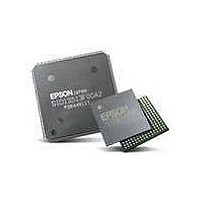
S1D13743F00A200 Epson, S1D13743F00A200 Datasheet - Page 131

S1D13743F00A200
Manufacturer Part Number
S1D13743F00A200
Description
LCD Drivers LCD CNTRL w/Embedded 464KB SRAM
Manufacturer
Epson
Datasheet
1.S1D13743F00A200.pdf
(134 pages)
Specifications of S1D13743F00A200
Maximum Clock Frequency
33 MHz, 68.59 MHz
Operating Supply Voltage
1.5 V
Maximum Operating Temperature
+ 85 C
Package / Case
QFP-20-144
Attached Touch Screen
No
Maximum Supply Current
74 mA
Minimum Operating Temperature
- 40 C
Lead Free Status / RoHS Status
Lead free / RoHS Compliant
Available stocks
Company
Part Number
Manufacturer
Quantity
Price
Company:
Part Number:
S1D13743F00A200
Manufacturer:
EPSON
Quantity:
5 690
Epson Research and Development
Vancouver Design Center
X70A-A-001-00
Hardware Functional Specification
Issue Date: 2010/05/18
• REG[04h] - change register name from “PLL M-Divider Register 0” to “PLL M-Divider
• REG[18h] - change minimum register value in note to 3
• REG[2Ah] - add note “For YUV 4:2:2 and YUV 4:2:0 settings, the width...”
• REG[2Ah] - add note “RGB 6:6:6 mode 2 and RGB 8:8:8 mode 2...”
• REG[34h] bits 6-4 - for 000b change FRM Mode Selected to Normal Mode, and add
• REG[36h] bit 7 - add note “While double buffering is enabled...”
• REG[36h] bit 6 - add note “While double buffering is enabled...”
• REG[48h] ~ REG[49h] - add note “Data read back from memory will be byte swapped”
• REG[56h] bit 1, fixed reference to REG[56h] bit 7 state, should be “Sleep mode can
• REG[56h] bit 0, fixed reference to REG[56h] bit 7 state, should be “Standby mode can
• REG[58h] bit 6 - swap “When this bit =...” descriptions
• REG[58h] bit 5 - rename bit to “VP OR’d with HDP Status (Read Only)”
• section 12 Intel 80, 16-bit Interface Color Formats - remove color from all Figures in
• section 13 YUV Timing - add format definition to this section
• section 13 YUV Timing - remove color from all Figures in section
• section 13.1 YUV 4:2:2 with Intel 80, 8-bit Interface, figure 13-1, correct U, V figure
• section 15 Display Data Format - Table 15-3 18-Bit Data Format (Non-Swapped,
• section 19.1.2 S1D13743 Register Settings for 352x416 TFT Panel - change REG[06h]
• section 19.1.2 S1D13742 Register Settings for 352x416 TFT Panel - add note “When a
• figure 4-1, changed “S1D13743 Proposed Pinout...” to “S1D13743 Pinout...”
• section 7.1.1 Input Clocks - Table 7-1 Clock Input Requirements (CLKI) - change fOSC
• section 7.3, corrected the formulas for HNDP (should be “REG[18h] bits 6-0” instead of
Revision 0.06
Register”
note “When the output is 24 bpp...”
also be controlled by the PWRSVE pin when REG[56h] bit 7 = 0b.” instead of “Sleep
mode can also be controlled by the PWRSVE pin when REG[56h] bit 7 = 1b.”
also be controlled by the PWRSVE pin when REG[56h] bit 7 = 1b.” instead of “Standby
mode can also be controlled by the PWRSVE pin when REG[56h] bit 7 = 0b.”
section
REG[14h] bit 7 = 0b), and Table 15-4 18-Bit Data Format (Swapped, REG[14h] bit 7 =
1b) change VD[23:18] value from Hi-Z to Low
value to F8h and REG[0Ah] value to 28h
window is setup for YUV data...”
Input clock frequency - PLL used for System Clock max to 66 MHz
“REG[18h] bits 5-0”), HSW (should be “REG[20h] bits 6-0” instead of “REG[20h] bits
5-0”), and VSW (should be “REG[24h] bits 5-0” instead of “REG[24h] bits 6-0”)
Revision 2.7
X70A-A-001-02
S1D13743
Page 131


