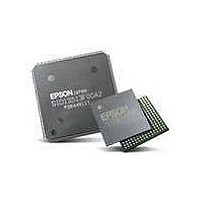
S1D13743F00A200 Epson, S1D13743F00A200 Datasheet - Page 32

S1D13743F00A200
Manufacturer Part Number
S1D13743F00A200
Description
LCD Drivers LCD CNTRL w/Embedded 464KB SRAM
Manufacturer
Epson
Datasheet
1.S1D13743F00A200.pdf
(134 pages)
Specifications of S1D13743F00A200
Maximum Clock Frequency
33 MHz, 68.59 MHz
Operating Supply Voltage
1.5 V
Maximum Operating Temperature
+ 85 C
Package / Case
QFP-20-144
Attached Touch Screen
No
Maximum Supply Current
74 mA
Minimum Operating Temperature
- 40 C
Lead Free Status / RoHS Status
Lead free / RoHS Compliant
Available stocks
Company
Part Number
Manufacturer
Quantity
Price
Company:
Part Number:
S1D13743F00A200
Manufacturer:
EPSON
Quantity:
5 690
- Current page: 32 of 134
- Download datasheet (3Mb)
Page 32
7.3.3 Definition of Transition Time to Hi-Z State
S1D13743
X70A-A-001-02
0.8 IOVDD
Tri state Output Cell
IOVDD
Volt
EN
A
½
IOVDD
Due to the difficulty of Hi-Z impedance measurement for high speed signals, transition
time from High/Low to Hi-Z specified as follows.
•
• Low to Hi-Z delay time: t
The functional model of a final stage of the Tri state Output Cell is shown in Figure 7-6:
“Definition of transition time to Hi-Z state”.
EN
High to Hi-Z delay time: t
turns to 0.8 x IOVDD (Pch-MOSFET is off). Total delay time to Hi-Z is calculated as follows:
MOSFET turns to 0.2 x IOVDD (Nch-MOSFET is off). Total delay time to Hi-Z is
calculated as follows:
Figure 7-6: Definition of Transition Time to Hi-Z State
t
pHZ
Internal logic delay + t
Internal logic delay + t
P
pHZ
Revision 2.7
pLZ
Time
,
delay time when a gate voltage of final stage of the Pch-MOSFET
0.2 IOVDD
, delay time when a gate voltage of final stage of the Nch-
IOVDD
pHZ
Volt
pHZ
(from High to Hi-Z)
to measure t
to measure t
(from High to Hi-Z)
½
IOVDD
VSS
IOVDD
EN
pHZ
pLZ
P
N
t
pLZ
Epson Research and Development
X
Hardware Functional Specification
N
Vancouver Design Center
Issue Date: 2010/05/18
Time
Related parts for S1D13743F00A200
Image
Part Number
Description
Manufacturer
Datasheet
Request
R

Part Number:
Description:
Display Modules & Development Tools S1D13743 Eval board
Manufacturer:
Epson

Part Number:
Description:
INK CARTRIDGE, T0803, EPSON, MAG
Manufacturer:
Epson
Datasheet:

Part Number:
Description:
INK CARTRIDGE, T0804, EPSON, YEL
Manufacturer:
Epson
Datasheet:

Part Number:
Description:
CXA1034M
Manufacturer:
EPSON Electronics
Datasheet:

Part Number:
Description:
Manufacturer:
EPSON Electronics
Datasheet:

Part Number:
Description:
Manufacturer:
EPSON Electronics
Datasheet:

Part Number:
Description:
Manufacturer:
EPSON Electronics
Datasheet:

Part Number:
Description:
Manufacturer:
EPSON Electronics
Datasheet:

Part Number:
Description:
RTC58321Real time clock module(4-bit I/O CONNECTION REAL TIME CLOCK MODULE)
Manufacturer:
EPSON Electronics
Datasheet:

Part Number:
Description:
SCI7661DC-DC Converter
Manufacturer:
EPSON Electronics
Datasheet:

Part Number:
Description:
Manufacturer:
EPSON Electronics
Datasheet:

Part Number:
Description:
Manufacturer:
EPSON Electronics
Datasheet:


