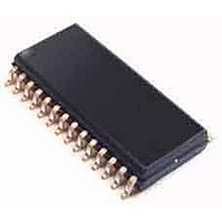
CS8427-CZZ Cirrus Logic Inc, CS8427-CZZ Datasheet - Page 29

CS8427-CZZ
Manufacturer Part Number
CS8427-CZZ
Description
Audio DSPs 96 kHz Digital Audio Transceiver
Manufacturer
Cirrus Logic Inc
Datasheet
1.CS8427-DZZ.pdf
(60 pages)
Specifications of CS8427-CZZ
Operating Supply Voltage
4.5 V to 5.5 V
Supply Current
6.3 mA to 76.6 mA
Operating Temperature Range
- 10 C to + 70 C
Mounting Style
SMD/SMT
Input Voltage
4.8 V to 5.8 V
Package / Case
TSSOP-28
Rohs Compliant
Yes
Supply Voltage Range
4.5V To 5.5V
Logic Case Style
TSSOP
No. Of Pins
28
Supply Voltage Max
5.5V
Supply Voltage Min
4.5V
Lead Free Status / RoHS Status
Lead free / RoHS Compliant
Available stocks
Company
Part Number
Manufacturer
Quantity
Price
Company:
Part Number:
CS8427-CZZ
Manufacturer:
CIRRUS
Quantity:
67
Part Number:
CS8427-CZZ
Manufacturer:
CIRRUS
Quantity:
20 000
MMR - Select AES3 receiver mono or stereo operation
MMT - Select AES3 transmitter mono or stereo operation
MMTCS - Select A or B channel status data to transmit in mono mode
MMTLR - Channel Selection for AES Transmitter mono mode
11.3 Data Flow Control (03h)
The Data Flow Control register configures the flow of audio data to/from the following blocks: Serial Audio Input Port,
Serial Audio Output Port, AES3 receiver, and AES3 transmitter. In conjunction with the Clock Source Control regis-
ter, multiple Receiver/Transmitter/Transceiver modes may be selected. The output data should be muted prior to
changing bits in this register to avoid transients.
TXOFF - AES3 Transmitter Output Driver Control
AESBP - AES3 bypass mode selection
TXD1:TXD0 - AES3 Transmitter Data Source
DS477F5
7
0
Default = ‘0’
0 - Normal stereo operation
1 - A and B subframes treated as consecutive samples of one channel of data. Data is duplicated to
Default = ‘0’
0 - Normal stereo operation
1 - Output either left or right channel inputs into consecutive subframe outputs (mono
Default = ‘0’
0 - Use channel A CS data for the A subframe and use channel B CS data for the B subframe
1 - Use the same CS data for both the A and B subframe outputs. If MMTLR = 0, use the
Default = ‘0’
0 - Use left channel input data for consecutive subframe outputs
1- Use right channel input data for consecutive subframe outputs
Default = ‘0
0 - AES3 transmitter output pin drivers normal operation
1 - AES3 transmitter output pin drivers drive to 0 V.
Default = ‘0’
0 - Normal operation
1 - Connect the AES3 transmitter driver input directly to the RXP pin, which becomes a normal TTL
threshold digital input. The transmitter clock (selecting using the OUTC bit in the Clock Source Control)
must be present for the bypass mode to work.
Default = ‘01’
00 - Reserved
01 - Serial audio input port
10 - AES3 receiver
11 - Reserved
both left and right parallel outputs of the AES receiver block. The input sample rate (Fsi) is doubled
compared to MMR=0
mode, left or right is determined by MMTLR bit)
left channel CS data. If MMTLR = 1, use the right channel CS data.
TXOFF
6
AESBP
5
TXD1
4
TXD0
3
SPD1
2
SPD0
1
CS8427
0
0
29


