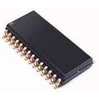
CS8427-CZZ Cirrus Logic Inc, CS8427-CZZ Datasheet - Page 32

CS8427-CZZ
Manufacturer Part Number
CS8427-CZZ
Description
Audio DSPs 96 kHz Digital Audio Transceiver
Manufacturer
Cirrus Logic Inc
Datasheet
1.CS8427-DZZ.pdf
(60 pages)
Specifications of CS8427-CZZ
Operating Supply Voltage
4.5 V to 5.5 V
Supply Current
6.3 mA to 76.6 mA
Operating Temperature Range
- 10 C to + 70 C
Mounting Style
SMD/SMT
Input Voltage
4.8 V to 5.8 V
Package / Case
TSSOP-28
Rohs Compliant
Yes
Supply Voltage Range
4.5V To 5.5V
Logic Case Style
TSSOP
No. Of Pins
28
Supply Voltage Max
5.5V
Supply Voltage Min
4.5V
Lead Free Status / RoHS Status
Lead free / RoHS Compliant
Available stocks
Company
Part Number
Manufacturer
Quantity
Price
Company:
Part Number:
CS8427-CZZ
Manufacturer:
CIRRUS
Quantity:
67
Part Number:
CS8427-CZZ
Manufacturer:
CIRRUS
Quantity:
20 000
SORES1:0 - Resolution of the output data on SDOUT and on the AES3 output
SOJUST - Justification of SDOUT data relative to OLRCK
SODEL - Delay of SDOUT data relative to OLRCK, for left-justified data formats
SOSPOL - OSCLK clock polarity
SOLRPOL - OLRCK clock polarity
11.7 Interrupt 1 Status (07h) (Read Only)
For all bits in this register, a “1” means the associated interrupt condition has occurred at least once since the register
was last read. A ”0” means the associated interrupt condition has NOT occurred since the last reading of the register.
Reading the register resets all bits to 0, unless the interrupt mode is set to level and the interrupt source is still true.
Status bits that are masked off in the associated mask register will always be “0” in this register. This register defaults
to 00h.
TSLIP - AES3 transmitter source data slip interrupt.
OSLIP - Serial audio output port data slip interrupt.
DETC - D to E C-buffer transfer interrupt.
EFTC - E to F C-buffer transfer interrupt.
RERR - A receiver error has occurred.
32
TSLIP
7
Default = ‘00’
00 - 24-bit resolution
01 - 20-bit resolution
10 - 16-bit resolution
11 - Direct copy of the received NRZ data from the AES3 receiver (including C, U, and
Default = ‘0’
0 - Left-justified
1 - Right-justified (master mode only)
Default = ‘0’
0 - MSB of SDOUT data occurs in the first OSCLK period after the OLRCK edge
1 - MSB of SDOUT data occurs in the second OSCLK period after the OLRCK edge
Default = ‘0’
0 - SDOUT transitions occur on falling edges of OSCLK
1 - SDOUT transitions occur on rising edges of OSCLK
Default = ‘0’
0 - SDOUT data is for the left channel when OLRCK is high
1 - SDOUT data is for the right channel when OLRCK is high
In data flows where OMCK, which clocks the AES3 transmitter, is asynchronous to the data source, this
bit will go high every time a data sample is dropped or repeated. When TCBL is an input, this bit will go
high on receipt of a new TCBL signal.
When the serial audio output port is in slave mode, and OLRCK is asynchronous to the port data source,
this bit will go high every time a data sample is dropped or repeated.
Indicates the completion of a D to E C-buffer transfer. See “Channel Status and User Data Buffer Man-
agement” on page 51 for more information.
Indicates the completion of a E to F C-buffer transfer. See “Channel Status and User Data Buffer Man-
agement” on page 51 for more information.
The Receiver Error register may be read to determine the nature of the error which caused the interrupt.
V bits, the time slot normally occupied by the P bit is used to indicate the location
of the block start, SDOUT pin only, serial audio output port clock must be derived
from the AES3 receiver recovered clock)
OSLIP
6
5
0
4
0
3
0
DETC
2
EFTC
1
CS8427
DS477F5
RERR
0


