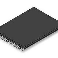
S29GL256P11TFI020 Spansion Inc., S29GL256P11TFI020 Datasheet - Page 53

S29GL256P11TFI020
Manufacturer Part Number
S29GL256P11TFI020
Description
Flash 3V 256Mb Mirrorbit lowest address110ns
Manufacturer
Spansion Inc.
Datasheet
1.S29GL128P11TFI020.pdf
(80 pages)
Specifications of S29GL256P11TFI020
Memory Type
NOR
Memory Size
256 Mbit
Access Time
110 ns
Data Bus Width
8 bit, 16 bit
Architecture
Uniform
Interface Type
Page-mode
Supply Voltage (max)
3.6 V
Supply Voltage (min)
2.7 V
Maximum Operating Current
50 mA
Mounting Style
SMD/SMT
Operating Temperature
+ 85 C
Package / Case
TSOP-56
Memory Configuration
128K X 16
Ic Interface Type
Parallel
Supply Voltage Range
2.7V To 3.6V
Memory Case Style
TSOP
No. Of Pins
56
Lead Free Status / RoHS Status
Lead free / RoHS Compliant
Lead Free Status / RoHS Status
Lead free / RoHS Compliant, Lead free / RoHS Compliant
Available stocks
Company
Part Number
Manufacturer
Quantity
Price
Company:
Part Number:
S29GL256P11TFI020
Manufacturer:
SPANSION
Quantity:
5 530
Company:
Part Number:
S29GL256P11TFI020
Manufacturer:
SPANSION
Quantity:
5 530
Company:
Part Number:
S29GL256P11TFI020
Manufacturer:
Spansion
Quantity:
135
11. Electrical Specifications
11.1
November 20, 2009 S29GL-P_00_A12
Absolute Maximum Ratings
Notes
1. Minimum DC voltage on input or I/Os is –0.5 V. During voltage transitions, inputs or I/Os may undershoot V
2. Minimum DC input voltage on pins A9 and ACC is -0.5V. During voltage transitions, A9 and ACC may overshoot V
3. No more than one output may be shorted to ground at a time. Duration of the short circuit should not be greater than one second.
4. Stresses above those listed under “Absolute Maximum Ratings” may cause permanent damage to the device. This is a stress rating only;
Description
Storage Temperature, Plastic Packages
Ambient Temperature with Power Applied
Voltage with Respect to Ground
Output Short Circuit Current (Note 3)
to 20 ns. See
V
of up to 20 ns. See
ns.
functional operation of the device at these or any other conditions above those indicated in the operational sections of this data sheet is not
implied. Exposure of the device to absolute maximum rating conditions for extended periods may affect device reliability.
CC
+ 2.0 V for periods up to 20 ns. See
Figure
Figure
11.1. Maximum DC voltage on input or I/Os is V
11.1. Maximum DC voltage on pins A9 and ACC is +12.5 V, which may overshoot to 14.0 V for periods up to 20
D a t a
+0 .8 V
+2.0 V
+0.5 V
+2.0 V
–0 .5 V
–2 .0 V
Figure 11.1 Maximum Negative Overshoot Waveform
Figure 11.2 Maximum Positive Overshoot Waveform
V
V
S29GL-P MirrorBit
CC
CC
Figure
S h e e t
11.2.
All Inputs and I/Os except as noted below
(Note 1)
V
V
A9 and ACC (Note 2)
CC
IO
20 ns
20 ns
(Note 1)
®
Flash Family
CC
20 n s
20 ns
+ 0.5 V. During voltage transitions inputs or I/Os may overshoot to
20 ns
20 ns
SS
–0.5 V to V
–0.5 V to +12.5 V
to –2.0 V for periods of up
–65°C to +150°C
–65°C to +125°C
–0.5 V to +4.0 V
–0.5V to +4.0V
SS
200 mA
Rating
to –2.0 V for periods
CC
+ 0.5 V
53


