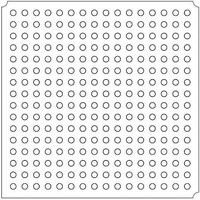
LFXP2-5E-5FTN256I Lattice, LFXP2-5E-5FTN256I Datasheet - Page 110

LFXP2-5E-5FTN256I
Manufacturer Part Number
LFXP2-5E-5FTN256I
Description
FPGA - Field Programmable Gate Array 5K LUTs 172 I/O Inst on DSP 1.2V -5 Spd
Manufacturer
Lattice
Datasheet
1.LFXP2-8E-5FTN256I.pdf
(341 pages)
Specifications of LFXP2-5E-5FTN256I
Number Of Macrocells
5000
Number Of Programmable I/os
172
Data Ram Size
169984
Supply Voltage (max)
1.26 V
Maximum Operating Temperature
+ 100 C
Minimum Operating Temperature
- 40 C
Mounting Style
SMD/SMT
Supply Voltage (min)
1.14 V
Package / Case
FTBGA-256
Number Of Logic Elements/cells
*
Number Of Labs/clbs
*
Total Ram Bits
169984
Number Of I /o
172
Number Of Gates
-
Voltage - Supply
1.14 V ~ 1.26 V
Mounting Type
*
Operating Temperature
-40°C ~ 100°C
Lead Free Status / RoHS Status
Lead free / RoHS Compliant
Available stocks
Company
Part Number
Manufacturer
Quantity
Price
Company:
Part Number:
LFXP2-5E-5FTN256I
Manufacturer:
Lattice
Quantity:
135
Company:
Part Number:
LFXP2-5E-5FTN256I
Manufacturer:
LATTICE
Quantity:
23
Company:
Part Number:
LFXP2-5E-5FTN256I
Manufacturer:
Lattice Semiconductor Corporation
Quantity:
10 000
Part Number:
LFXP2-5E-5FTN256I
Manufacturer:
LATTICE
Quantity:
20 000
- Current page: 110 of 341
- Download datasheet (10Mb)
Lattice Semiconductor
LVCMOS Buffer Configurations
All LVCMOS buffer have programmable pull, programmable drive and programmable slew configurations that can
be set in the software.
Bus Maintenance Circuit
Each pad has a weak pull-up, weak pull-down and weak buskeeper capability. The pull-up and pull-down settings
offer a fixed characteristic, which is useful in creating wired logic such as wired ORs. However, current can be
slightly higher than other options, depending on the signal state. The bus-keeper option latches the signal in the
last driven state, holding it at a valid level with minimal power dissipation. Users can also choose to turn off the bus
maintenance circuitry, minimizing power dissipation and input leakage. Note that in this case, it is important to
ensure that inputs are driven to a known state to avoid unnecessary power dissipation in the input buffer. The inter-
nal weak pull-up is enabled on all unused pins.
Programmable Drive
Each LVCMOS or LVTTL, as well as some of the referenced (SSTL and HSTL) output buffers, has a programmable
drive strength option. This option can be set for each I/O independently. The drive strength settings available are
2mA, 4mA, 6mA, 8mA, 12mA, 16mA and 20mA. Actual options available vary by the I/O voltage. The user must
consider the maximum allowable current per bank and the package thermal limit current when selecting the drive
strength. Table 8-6 shows the available drive settings for each of the output standards.
Table 8-6. Programmable Drive Values for Single-ended Buffers
Programmable Slew Rate
Each LVCMOS or LVTTL output buffer pin also has a programmable output slew rate control that can be configured
for either low noise or high-speed performance. Each I/O pin has an individual slew rate control. This allows
designers to specify slew rate control on a pin-by-pin basis. This slew rate control affects both the rising and falling
edges.
Open-Drain Control
All LVCMOS and LVTTL output buffers can be configured to function as open drain outputs. The user can imple-
ment an open drain output by turning on the OPENDRAIN attribute in the software.
Differential SSTL and HSTL support
The single-ended driver associated with the complementary ‘C’ pad can optionally be driven by the complement of
the data that drives the single-ended driver associated with the true pad. This allows a pair of single-ended drivers
to be used to drive complementary outputs with the lowest possible skew between the signals. This is used for driv-
ing complementary SSTL and HSTL signals (as required by the differential SSTL and HSTL clock inputs on syn-
HSTL15_I
HSTL18_I
SSTL25_I
SSTL25_II
SSTL18_II
LVCMOS12
LVCMOS15
LVCMOS18
LVCMOS25
LVCMOS33
LVTTL
Single Ended I/O Standard
8-6
Programmable Drive (mA)
4, 8, 12, 16, 20
4, 8, 12, 16, 20
4, 8, 12, 16, 20
4, 8, 12, 16
16, 20
8, 12
8, 12
8, 12
4, 8
2, 6
4, 8
LatticeXP2 sysIO Usage Guide
Related parts for LFXP2-5E-5FTN256I
Image
Part Number
Description
Manufacturer
Datasheet
Request
R

Part Number:
Description:
FPGA - Field Programmable Gate Array 5K LUTs 146I/O Inst- on DSP 1.2V -5 Spd
Manufacturer:
Lattice
Datasheet:

Part Number:
Description:
FPGA - Field Programmable Gate Array 5K LUTs 172I/O Inst- on DSP 1.2V -5 Spd
Manufacturer:
Lattice
Datasheet:

Part Number:
Description:
FPGA - Field Programmable Gate Array 5K LUTs 100 I/O Inst on DSP 1.2V -5 Spd
Manufacturer:
Lattice
Datasheet:

Part Number:
Description:
FPGA - Field Programmable Gate Array 5K LUTs 100I/O Inst- on DSP 1.2V -5 Spd
Manufacturer:
Lattice
Datasheet:
Part Number:
Description:
FPGA LatticeXP2 Family 5000 Cells Flash Technology 1.2V 256-Pin FTBGA
Manufacturer:
LATTICE SEMICONDUCTOR
Datasheet:
Part Number:
Description:
FPGA LatticeXP2 Family 5000 Cells Flash Technology 1.2V 256-Pin FTBGA
Manufacturer:
LATTICE SEMICONDUCTOR
Datasheet:

Part Number:
Description:
IC DSP 5KLUTS 100I/O 144TQFP
Manufacturer:
Lattice
Datasheet:

Part Number:
Description:
IC DSP 5KLUTS 86I/O 132CSBGA
Manufacturer:
Lattice
Datasheet:

Part Number:
Description:
IC DSP 5KLUTS 86I/O 132CSBGA
Manufacturer:
Lattice
Datasheet:

Part Number:
Description:
IC DSP 5KLUTS 146I/O 208PQFP
Manufacturer:
Lattice
Datasheet:

Part Number:
Description:
IC DSP 5KLUTS 146I/O 208PQFP
Manufacturer:
Lattice
Datasheet:

Part Number:
Description:
IC DSP 5KLUTS 172I/O 256FTBGA
Manufacturer:
Lattice
Datasheet:

Part Number:
Description:
IC FPGA 5KLUTS 86I/O 132-BGA
Manufacturer:
Lattice
Datasheet:

Part Number:
Description:
IC FPGA 5KLUTS 86I/O 132-BGA
Manufacturer:
Lattice
Datasheet:

Part Number:
Description:
IC FPGA 5KLUTS 86I/O 132-BGA
Manufacturer:
Lattice
Datasheet:


