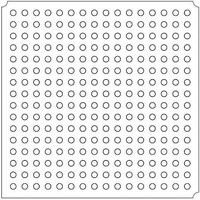
LFXP2-5E-5FTN256I Lattice, LFXP2-5E-5FTN256I Datasheet - Page 283

LFXP2-5E-5FTN256I
Manufacturer Part Number
LFXP2-5E-5FTN256I
Description
FPGA - Field Programmable Gate Array 5K LUTs 172 I/O Inst on DSP 1.2V -5 Spd
Manufacturer
Lattice
Datasheet
1.LFXP2-8E-5FTN256I.pdf
(341 pages)
Specifications of LFXP2-5E-5FTN256I
Number Of Macrocells
5000
Number Of Programmable I/os
172
Data Ram Size
169984
Supply Voltage (max)
1.26 V
Maximum Operating Temperature
+ 100 C
Minimum Operating Temperature
- 40 C
Mounting Style
SMD/SMT
Supply Voltage (min)
1.14 V
Package / Case
FTBGA-256
Number Of Logic Elements/cells
*
Number Of Labs/clbs
*
Total Ram Bits
169984
Number Of I /o
172
Number Of Gates
-
Voltage - Supply
1.14 V ~ 1.26 V
Mounting Type
*
Operating Temperature
-40°C ~ 100°C
Lead Free Status / RoHS Status
Lead free / RoHS Compliant
Available stocks
Company
Part Number
Manufacturer
Quantity
Price
Company:
Part Number:
LFXP2-5E-5FTN256I
Manufacturer:
Lattice
Quantity:
135
Company:
Part Number:
LFXP2-5E-5FTN256I
Manufacturer:
LATTICE
Quantity:
23
Company:
Part Number:
LFXP2-5E-5FTN256I
Manufacturer:
Lattice Semiconductor Corporation
Quantity:
10 000
Part Number:
LFXP2-5E-5FTN256I
Manufacturer:
LATTICE
Quantity:
20 000
- Current page: 283 of 341
- Download datasheet (10Mb)
LatticeXP2 sysCONFIG
Usage Guide
June 2009
Technical Note TN1141
Introduction
The memory in the LatticeXP2™ FPGAs is built using Flash cells, along with SRAM cells, so that configuration
memory can be loaded automatically at power-up, or at any time the user wishes to update the device. In addition
to “instant-on” capability, on-chip Flash memory greatly increases design security by getting rid of the external con-
figuration bitstream; while maintaining the ease of use and reprogrammability of an SRAM-based FPGA.
The LatticeXP2 supports the use of an encryption key to protect the contents of the Flash memory for additional
security. The LatticeXP2 also supports the use of a One-Time-Programmable (OTP) feature to protect the Flash
memory from being erased or re-programmed.
While an external device is not required, the LatticeXP2 does support several external configuration modes. The
available external configuration modes are:
• Slave SPI
• Master SPI
• ispJTAG™ (1149.1 interface)
This guide will cover all the configuration options available for the LatticeXP2.
Programming Overview
The LatticeXP2 contains two types of memory, SRAM and Flash (refer to Figure 14-1). SRAM contains the FPGA
configuration, essentially the “fuses” that define the circuit connections; Flash provides an internal storage space
for the configuration data.
The LatticeXP2 also contains additional Flash memory area and that is designated for Tag memory and User Flash
memory. The Tag memory is a scratch pad memory that is available to the user for storage of mission critical data,
board serialization, revision information, programmed pattern identification, or other information. The User Flash
memory is available to provide a back up the contents of the EBR RAM modules if the user desires. These func-
tions will be discussed in more detail in later sections of this document.
The SRAM can be configured using JTAG, the external Master SPI port, or by using the data stored in on-chip
Flash. The configuration process consists of SRAM initialization (clear the RAM and the address pointers), loading
the SRAM with the configuration data, and setting the FPGA into user mode (waking up the FPGA).
On-chip Flash can be programmed by using JTAG or by using the external Slave SPI port. JTAG Flash program-
ming can be performed any time the device is powered up. The Slave SPl port uses the sysCONFIG™ pins and
can program the Flash directly or in the background. Direct programming takes place during config mode, back-
ground programming during user mode. The FPGA enters config mode at power up, when the PROGRAMN pin is
pulled low, or when a refresh command is issued via JTAG; it enters user mode when it wakes up, i.e. when the
device begins running user code. These two programming modes, direct and background, will be referred to in this
document as Flash Direct and Flash Background.
© 2009 Lattice Semiconductor Corp. All Lattice trademarks, registered trademarks, patents, and disclaimers are as listed at www.latticesemi.com/legal. All other brand
or product names are trademarks or registered trademarks of their respective holders. The specifications and information herein are subject to change without notice.
www.latticesemi.com
14-1
tn1141_01.6
Related parts for LFXP2-5E-5FTN256I
Image
Part Number
Description
Manufacturer
Datasheet
Request
R

Part Number:
Description:
FPGA - Field Programmable Gate Array 5K LUTs 146I/O Inst- on DSP 1.2V -5 Spd
Manufacturer:
Lattice
Datasheet:

Part Number:
Description:
FPGA - Field Programmable Gate Array 5K LUTs 172I/O Inst- on DSP 1.2V -5 Spd
Manufacturer:
Lattice
Datasheet:

Part Number:
Description:
FPGA - Field Programmable Gate Array 5K LUTs 100 I/O Inst on DSP 1.2V -5 Spd
Manufacturer:
Lattice
Datasheet:

Part Number:
Description:
FPGA - Field Programmable Gate Array 5K LUTs 100I/O Inst- on DSP 1.2V -5 Spd
Manufacturer:
Lattice
Datasheet:
Part Number:
Description:
FPGA LatticeXP2 Family 5000 Cells Flash Technology 1.2V 256-Pin FTBGA
Manufacturer:
LATTICE SEMICONDUCTOR
Datasheet:
Part Number:
Description:
FPGA LatticeXP2 Family 5000 Cells Flash Technology 1.2V 256-Pin FTBGA
Manufacturer:
LATTICE SEMICONDUCTOR
Datasheet:

Part Number:
Description:
IC DSP 5KLUTS 100I/O 144TQFP
Manufacturer:
Lattice
Datasheet:

Part Number:
Description:
IC DSP 5KLUTS 86I/O 132CSBGA
Manufacturer:
Lattice
Datasheet:

Part Number:
Description:
IC DSP 5KLUTS 86I/O 132CSBGA
Manufacturer:
Lattice
Datasheet:

Part Number:
Description:
IC DSP 5KLUTS 146I/O 208PQFP
Manufacturer:
Lattice
Datasheet:

Part Number:
Description:
IC DSP 5KLUTS 146I/O 208PQFP
Manufacturer:
Lattice
Datasheet:

Part Number:
Description:
IC DSP 5KLUTS 172I/O 256FTBGA
Manufacturer:
Lattice
Datasheet:

Part Number:
Description:
IC FPGA 5KLUTS 86I/O 132-BGA
Manufacturer:
Lattice
Datasheet:

Part Number:
Description:
IC FPGA 5KLUTS 86I/O 132-BGA
Manufacturer:
Lattice
Datasheet:

Part Number:
Description:
IC FPGA 5KLUTS 86I/O 132-BGA
Manufacturer:
Lattice
Datasheet:


