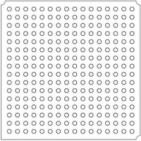
LFXP2-5E-5FTN256I Lattice, LFXP2-5E-5FTN256I Datasheet - Page 287

LFXP2-5E-5FTN256I
Manufacturer Part Number
LFXP2-5E-5FTN256I
Description
FPGA - Field Programmable Gate Array 5K LUTs 172 I/O Inst on DSP 1.2V -5 Spd
Manufacturer
Lattice
Datasheet
1.LFXP2-8E-5FTN256I.pdf
(341 pages)
Specifications of LFXP2-5E-5FTN256I
Number Of Macrocells
5000
Number Of Programmable I/os
172
Data Ram Size
169984
Supply Voltage (max)
1.26 V
Maximum Operating Temperature
+ 100 C
Minimum Operating Temperature
- 40 C
Mounting Style
SMD/SMT
Supply Voltage (min)
1.14 V
Package / Case
FTBGA-256
Number Of Logic Elements/cells
*
Number Of Labs/clbs
*
Total Ram Bits
169984
Number Of I /o
172
Number Of Gates
-
Voltage - Supply
1.14 V ~ 1.26 V
Mounting Type
*
Operating Temperature
-40°C ~ 100°C
Lead Free Status / RoHS Status
Lead free / RoHS Compliant
Available stocks
Company
Part Number
Manufacturer
Quantity
Price
Company:
Part Number:
LFXP2-5E-5FTN256I
Manufacturer:
Lattice
Quantity:
135
Company:
Part Number:
LFXP2-5E-5FTN256I
Manufacturer:
LATTICE
Quantity:
23
Company:
Part Number:
LFXP2-5E-5FTN256I
Manufacturer:
Lattice Semiconductor Corporation
Quantity:
10 000
Part Number:
LFXP2-5E-5FTN256I
Manufacturer:
LATTICE
Quantity:
20 000
- Current page: 287 of 341
- Download datasheet (10Mb)
Lattice Semiconductor
LatticeXP2 sysCONFIG Usage Guide
CCLK
CCLK is a dual-purpose bi-directional pin; direction depends on whether a Master or Slave mode is selected. If a
Master mode is selected, the CCLK pin will become an output pin; otherwise CCLK is an input pin.
If the CCLK pin becomes an output, the internal programmable oscillator is connected to the CCLK and is driven
out to slave devices. CCLK will stop 100 to 500 clock cycles after the DONE pin is brought high and the device
wake-up sequence completed. The extra clock cycles ensure that enough clocks are provided to wake-up other
devices in the chain. When stopped, CCLK becomes an input (tri-stated output). CCLK will restart (become an out-
put) on the next configuration initialization sequence.
CSSPIN
The CSSPIN pin is a dual-purpose output pin with a weak pull-up. The CSSPIN is an active low chip select to an
external SPI flash when used with the Master SPI mode. The CSSPIN pin becomes a dedicated pin if the CFG0 pin
is set to 0 (not in SDM mode). When the CFG0 pin is set to 1 then CSSPIN becomes a general purpose I/O pin
available to the user.
If the CFG0 is set to 0 then this pin should be driven high unless the Master SPI mode is selected to avoid conten-
tion between the Master and Slave SPI modes.
CSSPISN
The CSSPISN pin is a dual-purpose input pin with a weak pull-up. The CSSPISN is an active low chip select to the
internal SPI interface and is used with the Slave SPI mode.
If the CSSPISN is driven low while in the middle of Master SPI port activity the Master SPI shall be disabled and
the Slave SPI interface activated.
The PERSISTENT preference must be set to ON in order to preserve this pin as CSSPISN and allow access to the
Slave SPI interface. The PERSISTENT preference will be set by the software automatically when the user sets the
SLAVE_SPI_PORT option in the Design Planner.
SISPI
The SISPI pin is a dual-purpose bi-directional pin; direction depends upon whether a Master or Slave mode is
active. The SISPI is the Input data pin when using the Slave SPI mode and is the Output data pin when using the
Master SPI mode.
The PERSISTENT preference must be set to ON in order to preserve this pin as SISPI and allow access to the
Slave SPI interface. The PERSISTENT preference will be set by the software automatically when the user sets the
SLAVE_SPI_PORT option in the Design Planner.
SOSPI
The SOSPI pin is a dual-purpose bi-directional pin; direction depends upon whether a Master or Slave mode is
active. The SOSPI is the Input data pin when using the Master SPI mode and is the Output data pin when using the
Slave SPI mode.
The PERSISTENT preference must be set to ON in order to preserve this pin as SOSPI and allow access to the
Slave SPI interface. The PERSISTENT preference will be set by the software automatically when the user sets the
SLAVE_SPI_PORT option in the Design Planner.
14-5
Related parts for LFXP2-5E-5FTN256I
Image
Part Number
Description
Manufacturer
Datasheet
Request
R

Part Number:
Description:
FPGA - Field Programmable Gate Array 5K LUTs 146I/O Inst- on DSP 1.2V -5 Spd
Manufacturer:
Lattice
Datasheet:

Part Number:
Description:
FPGA - Field Programmable Gate Array 5K LUTs 172I/O Inst- on DSP 1.2V -5 Spd
Manufacturer:
Lattice
Datasheet:

Part Number:
Description:
FPGA - Field Programmable Gate Array 5K LUTs 100 I/O Inst on DSP 1.2V -5 Spd
Manufacturer:
Lattice
Datasheet:

Part Number:
Description:
FPGA - Field Programmable Gate Array 5K LUTs 100I/O Inst- on DSP 1.2V -5 Spd
Manufacturer:
Lattice
Datasheet:
Part Number:
Description:
FPGA LatticeXP2 Family 5000 Cells Flash Technology 1.2V 256-Pin FTBGA
Manufacturer:
LATTICE SEMICONDUCTOR
Datasheet:
Part Number:
Description:
FPGA LatticeXP2 Family 5000 Cells Flash Technology 1.2V 256-Pin FTBGA
Manufacturer:
LATTICE SEMICONDUCTOR
Datasheet:

Part Number:
Description:
IC DSP 5KLUTS 100I/O 144TQFP
Manufacturer:
Lattice
Datasheet:

Part Number:
Description:
IC DSP 5KLUTS 86I/O 132CSBGA
Manufacturer:
Lattice
Datasheet:

Part Number:
Description:
IC DSP 5KLUTS 86I/O 132CSBGA
Manufacturer:
Lattice
Datasheet:

Part Number:
Description:
IC DSP 5KLUTS 146I/O 208PQFP
Manufacturer:
Lattice
Datasheet:

Part Number:
Description:
IC DSP 5KLUTS 146I/O 208PQFP
Manufacturer:
Lattice
Datasheet:

Part Number:
Description:
IC DSP 5KLUTS 172I/O 256FTBGA
Manufacturer:
Lattice
Datasheet:

Part Number:
Description:
IC FPGA 5KLUTS 86I/O 132-BGA
Manufacturer:
Lattice
Datasheet:

Part Number:
Description:
IC FPGA 5KLUTS 86I/O 132-BGA
Manufacturer:
Lattice
Datasheet:

Part Number:
Description:
IC FPGA 5KLUTS 86I/O 132-BGA
Manufacturer:
Lattice
Datasheet:


