MMA7455LT Freescale Semiconductor, MMA7455LT Datasheet - Page 26
MMA7455LT
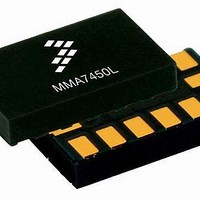
Manufacturer Part Number
MMA7455LT
Description
Board Mount Accelerometers 3-AXIS DIGITAL 2 4 8G
Manufacturer
Freescale Semiconductor
Datasheet
1.MMA7455LT.pdf
(35 pages)
Specifications of MMA7455LT
Sensing Axis
X, Y, Z
Acceleration
2 g, 4 g, 8 g
Supply Voltage (max)
3.6 V
Supply Voltage (min)
2.4 V
Supply Current
400 uA
Maximum Operating Temperature
+ 85 C
Minimum Operating Temperature
- 40 C
Sensitivity
64 LSB/g
Package / Case
LGA-14
Output Type
Digital
Acceleration Range
± 2g, ± 4g, ± 8g
No. Of Axes
3
Sensor Case Style
LGA
No. Of Pins
14
Supply Voltage Range
2.4V To 3.6V
Operating Temperature Range
-40°C To +85°C
Filter Terminals
SMD
Rohs Compliant
Yes
Ic Interface Type
I2C, SPI
Lead Free Status / RoHS Status
Lead free / RoHS Compliant
Available stocks
Company
Part Number
Manufacturer
Quantity
Price
Company:

Part Number:
MMA7455LT
Manufacturer:
FREESCALE
Quantity:
18 300
Part Number:
MMA7455LT
Manufacturer:
FREESCALE
Quantity:
20 000


Table 12. Configuring the Interrupt settings using Register $18 with INTREG[1:0] bits
$17: Interrupt Latch Reset (Read/Write)
CLR_INT1
CLR_INT2
00: INT1 Register is detecting Level while INT2 is detecting Pulse.
01: INT1 Register is detecting Pulse while INT2 is detecting Level.
10: INT1 Register is detecting a Single Pulse and INT2 is detecting Single Pulse (if 2
time window and second time window > 0 then INT2 will detect the double pulse only.
INTPIN: INT1 pin is routed to INT1 bit in Detection Source Register ($0A) and INT2 pin is routed to INT2 bit in Detection Source
Register ($0A).
INTPIN: INT2 pin is routed to INT1 bit in Detection Source Register ($0A) and INT1 pin is routed to INT2 bit in Detection Source
Register ($0A).
XDA
1: X-axis is disabled for detection.
0: X-axis is enabled for detection.
YDA
1: Y-axis is disabled for detection.
0: Y-axis is enabled for detection.
ZDA
1: Z-axis is disabled for detection.
0: Z-axis is enabled for detection.
$19: Control 2 (Read/Write)
LDPL
0: Level detection polarity is positive and detecting condition
is OR 3 axes.
1: Level detection polarity is negative detecting condition is
AND 3 axes.
$18 Control 1 (Read/Write)
26
MMA7455L
DFBW
D7
D7
D7
--
0
0
0
INTREG[1:0]
1: Clear “INT1” and LDX/LDY/LDZ or PDX/PDY/PDZ bits in Detection Source Register ($0A) depending on
Control1($18) INTREG[1:0] setting.
0: Do not clear “INT1” LDX/LDY/LDZ or PDX/PDY/PDZ bits in Detection Source Register ($0A)
1: Clear “INT2” and LDX/LDY/LDZ or PDX/PDY/PDZ bits in Detection Source Register ($0A) depending on
Control1($18) INTREG[1:0] setting.
0: Do not clear “INT2” and LDX/LDY/LDZ or PDX/PDY/PDZ bits in Detection Source Register ($0A).
00
01
10
THOPT
D6
D6
D6
--
0
0
0
ZDA
D5
D5
D5
--
0
0
0
Single Pulse detection
“INT1” Register Bit
Pulse Detection
Level detection
YDA
D4
D4
D4
--
0
0
0
XDA
D3
D3
D3
0
--
0
0
THOPT (This bit is valid for level detection only, not valid
DFBW
0: Digital filter band width is 62.5 Hz
1: Digital filter band width is 125 Hz
PDPL
0: Pulse detection polarity is positive and detecting condition
is OR 3 axes.
1: Pulse detection polarity is negative and detecting condition
is AND 3 axes.
DRVO
0: Standard drive strength on SDA/SDO pin
1: Strong drive strength on SDA/SDO pin
0: Threshold value is absolute only
1: Integer value is available.
for pulse detection)
INTREG[1]
DRVO
D2
D2
D2
0
--
0
0
nd
Time Window = 0) or if there is a latency
INTREG[0]
CLR_INT2
Single or Double Pulse Detection
PDPL
D1
D1
D1
0
0
0
“INT2” Register Bit
Pulse Detection
Level Detection
CLR_INT1
Freescale Semiconductor
INTPIN
LDPL
D0
D0
D0
0
0
0
Function
Function
Function
Default
Default
Default
Bit
Bit
Bit
Sensors
Related parts for MMA7455LT
Image
Part Number
Description
Manufacturer
Datasheet
Request
R

Part Number:
Description:
IC ACCELEROMETER 3AXIS 16QFN
Manufacturer:
Freescale Semiconductor
Datasheet:

Part Number:
Description:
SENSOR ACCEL Z-AX +/-1.5G 16SOIC
Manufacturer:
Freescale Semiconductor
Datasheet:
Part Number:
Description:
IC SENSOR ACCEL +/-200G 16-SOIC
Manufacturer:
Freescale Semiconductor
Datasheet:
Part Number:
Description:
SENS ACCEL X-AXIS +/-50G 16-SOIC
Manufacturer:
Freescale Semiconductor
Datasheet:
Part Number:
Description:
SENSOR ACCEL Z-AXIS 1.5G 16-SOIC
Manufacturer:
Freescale Semiconductor
Datasheet:
Part Number:
Description:
IC ACCELEROMETER Z AXIS 16-SOIC
Manufacturer:
Freescale Semiconductor
Datasheet:
Part Number:
Description:
IC ACCELEROMETER Z AXIS 16-SOIC
Manufacturer:
Freescale Semiconductor
Datasheet:
Part Number:
Description:
SENSOR ACCEL Z-AXIS 1.5G 16-SOIC
Manufacturer:
Freescale Semiconductor
Datasheet:
Part Number:
Description:
SENSOR ACCEL X-AXIS+/-40G 16SOIC
Manufacturer:
Freescale Semiconductor
Datasheet:
Part Number:
Description:
SENSOR ACCEL X-AXIS 50G 16-SOIC
Manufacturer:
Freescale Semiconductor
Datasheet:

Part Number:
Description:
Manufacturer:
Freescale Semiconductor, Inc
Datasheet:
Part Number:
Description:
Manufacturer:
Freescale Semiconductor, Inc
Datasheet:
Part Number:
Description:
Manufacturer:
Freescale Semiconductor, Inc
Datasheet:
Part Number:
Description:
Manufacturer:
Freescale Semiconductor, Inc
Datasheet:
Part Number:
Description:
Manufacturer:
Freescale Semiconductor, Inc
Datasheet: