BSC0901NS Infineon Technologies, BSC0901NS Datasheet
BSC0901NS
Specifications of BSC0901NS
Available stocks


Related parts for BSC0901NS

BSC0901NS Summary of contents
Page 1
... OptiMOS™ BSC0901NS 2.0, 2011-03-01 Final & ...
Page 2
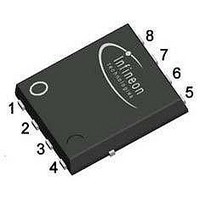
... Type Package BSC0901NS PG-TDSON-8 1) J-STD20 and JESD22 Final Data Sheet @ V =4 for target applications Unit V mΩ Marking 0901NS 1 OptiMOS™ Power-MOSFET BSC0901NS Related Links IFX OptiMOS webpage IFX OptiMOS product brief IFX OptiMOS spice models IFX Design tools 2.0, 2011-03-01 ...
Page 3
... Symbol Values Min. Typ thJC - - thJA 2 (one layer, 70 µm thick) copper area for drain connection. 2 OptiMOS™ Power-MOSFET BSC0901NS Unit Note / Test Condition =25 ° = =100 ° =4 =25 ° =4 =100 °C ...
Page 4
... GSS R - 1.9 DS(on 140 fs Symbol Values Min. Typ 2800 iss C - 960 oss C - 140 rss t - 5.4 d(on 6 d(off 4 OptiMOS™ Power-MOSFET BSC0901NS Electrical characteristics Unit Note / Test Condition Max =1 2 =250 µ µA = =25 ° 100 = =125 ° 100 nA = 2.4 mΩ =4.5 V, ...
Page 5
... Reverse recovery charge Final Data Sheet 1) Symbol Values Min. Typ 4.6 g( 2.4 plateau g(sync oss Symbol Values Min. Typ S,pulse OptiMOS™ Power-MOSFET BSC0901NS Electrical characteristics Unit Note / Test Condition Max = = 10V = Unit Note / Test Condition Max =25 °C C 276 = =25 ° ...
Page 6
... Electrical characteristics diagrams Table 8 1 Power dissipation tot C Table 9 3 Safe operating area T =25 ° =f =25 °C; D=0; parameter Final Data Sheet 2 Drain current I =f(T ); parameter Max. transient thermal impedance Z =f(t ); parameter: D=t p (thJC OptiMOS™ Power-MOSFET BSC0901NS Electrical characteristics diagrams : 2.0, 2011-03-01 ...
Page 7
... Typ. output characteristics I =f =25 °C; parameter Table 11 7 Typ. transfer characteristics I =f(VGS); |V |>2 DS(on)max Final Data Sheet T =25 °C 6 Typ. drain-source on-state resistance C R =f(I GS DS(on) 8 Typ. forward transconductance g =f OptiMOS™ Power-MOSFET BSC0901NS Electrical characteristics diagrams ); T =25 °C; parameter =25 °C j 2.0, 2011-03-01 ...
Page 8
... Table 12 9 Drain-source on-state resistance =10 V DS(on Table 13 11 Typ. capacitances C=f f=1 MHz DS GS Final Data Sheet OptiMOS™ Power-MOSFET Electrical characteristics diagrams 10 Typ. gate threshold voltage V =f =250 µA GS(th Forward characteristics of reverse diode I =f(V ); parameter BSC0901NS 2.0, 2011-03-01 ...
Page 9
... Table 14 13 Avalanche characteristics =25 Ω; parameter =f Table 15 15 Drain-source breakdown voltage V =f BR(DSS Final Data Sheet 14 Typ. gate charge V =f(Q j(start) GS gate 16 Gate charge waveforms 8 OptiMOS™ Power-MOSFET BSC0901NS Electrical characteristics diagrams ); I =30 A pulsed; parameter 2.0, 2011-03-01 ...
Page 10
... Package outline Figure 1 Outlines PG-TDSON-8, dimensions in mm/inches Final Data Sheet OptiMOS™ Power-MOSFET 9 BSC0901NS Package outline 2.0, 2011-03-01 ...
Page 11
... Figure 2 Outlines PG-TDSON-8 tape, dimension in mm/inches Final Data Sheet OptiMOS™ Power-MOSFET 10 BSC0901NS Package outline 2.0, 2011-03-01 ...
Page 12
... Life support devices or systems are intended to be implanted in the human body or to support and/or maintain and sustain and/or protect human life. If they fail reasonable to assume that the health of the user or other persons may be endangered. Final Data Sheet OptiMOS™ Power-MOSFET erratum@infineon.com 11 BSC0901NS Revision History 2.0, 2011-03-01 ...