BSC0901NS Infineon Technologies, BSC0901NS Datasheet - Page 3
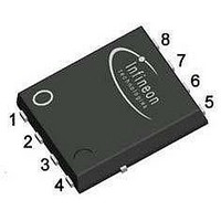
BSC0901NS
Manufacturer Part Number
BSC0901NS
Description
MOSFET N-CH 30V 100A 8TDSON
Manufacturer
Infineon Technologies
Series
OptiMOS™r
Datasheet
1.BSC0901NS.pdf
(12 pages)
Specifications of BSC0901NS
Input Capacitance (ciss) @ Vds
2800pF @ 15V
Fet Type
MOSFET N-Channel, Metal Oxide
Fet Feature
Logic Level Gate
Rds On (max) @ Id, Vgs
1.9 mOhm @ 30A, 10V
Drain To Source Voltage (vdss)
30V
Current - Continuous Drain (id) @ 25° C
100A
Vgs(th) (max) @ Id
2.2V @ 250µA
Gate Charge (qg) @ Vgs
44nC @ 10V
Power - Max
69W
Mounting Type
Surface Mount
Package / Case
8-PowerTDFN
Transistor Polarity
N-Channel
Resistance Drain-source Rds (on)
1.6 mOhms
Forward Transconductance Gfs (max / Min)
140 S, 70 S
Drain-source Breakdown Voltage
30 V
Gate-source Breakdown Voltage
20 V
Continuous Drain Current
100 A
Power Dissipation
2.5 W
Maximum Operating Temperature
+ 150 C
Mounting Style
SMD/SMT
Minimum Operating Temperature
- 55 C
Lead Free Status / RoHS Status
Lead free / RoHS Compliant
Other names
BSC0901NSTR
Available stocks
Company
Part Number
Manufacturer
Quantity
Price

Part Number:
BSC0901NS
Manufacturer:
INFINEON/英飞凌
Quantity:
20 000
Part Number:
BSC0901NSATMA1
Manufacturer:
INFINEON/英飞凌
Quantity:
20 000
Part Number:
BSC0901NSI
Manufacturer:
INFINEON/英飞凌
Quantity:
20 000
Part Number:
BSC0901NSIATMA1
Manufacturer:
INFINEON/英飞凌
Quantity:
20 000


2
at
Table 2
Parameter
Continuous drain current
Pulsed drain current
Avalanche current, single pulse
Avalanche energy, single pulse
Gate source voltage
Power dissipation
Operating and storage temperature
IEC climatic category; DIN IEC 68-1
1) Device on 40 mm x 40 mm x 1.5 mm epoxy PCB FR4 with 6 cm
2)
3) See figure 13 for more detailed information
3
Table 3
Parameter
Thermal resistance, junction - case
Device on PCB
1) Device on 40 mm x 40 mm x 1.5 mm epoxy PCB FR4 with 6 cm
Final Data Sheet
T
PCB is vertical in still air.
PCB is vertical in still air
j
See figure 3 for more detailed information
= 25 °C, unless otherwise specified.
Maximum ratings
Maximum ratings
Thermal characteristics
Thermal characteristics
2)
3)
Symbol
R
R
Symbol
I
I
I
E
V
P
T
D
D,pulse
AS
thJC
thJA
j
AS
GS
tot
,T
stg
Min.
-
-
-
Min.
-
-
-
-
-
-
-
-
-20
-
-
-55
55/150/56
2
Typ.
-
-
-
Typ. Max.
-
-
-
-
-
-
-
-
-
-
-
-
2
2
Values
(one layer, 70 µm thick) copper area for drain connection.
Values
(one layer, 70 µm thick) copper area for drain connection.
100
94
100
84
28
400
50
80
20
69
2.5
150
Max.
1.8
20
50
OptiMOS™ Power-MOSFET
Unit
A
mJ
V
W
°C
Unit
K/W
Note / Test Condition
V
V
V
V
V
R
T
I
T
T
D
C
C
A
GS
GS
GS
GS
GS
thJA
=50 A,R
=25 °C
=25 °C
=25 °C, R
=10 V, T
=10 V, T
=4.5 V, T
=4.5 V, T
=10 V, T
Note /
Test Condition
top
6 cm
=50 K/W
2
GS
2.0, 2011-03-01
cooling area
BSC0901NS
=25 Ω
thJA
C
C
A
C
C
=25 °C
=100 °C
=25 °C,
1)
=25 °C
=100 °C
)
=50 K/W
1)
1)
)
Related parts for BSC0901NS
Image
Part Number
Description
Manufacturer
Datasheet
Request
R

Part Number:
Description:
Manufacturer:
Infineon Technologies AG
Datasheet:
Part Number:
Description:
Manufacturer:
Infineon Technologies AG
Datasheet:
Part Number:
Description:
Manufacturer:
Infineon Technologies AG
Datasheet:
Part Number:
Description:
Manufacturer:
Infineon Technologies AG
Datasheet:
Part Number:
Description:
Manufacturer:
Infineon Technologies AG
Datasheet:
Part Number:
Description:
Manufacturer:
Infineon Technologies AG
Datasheet:
Part Number:
Description:
Manufacturer:
Infineon Technologies AG
Datasheet:
Part Number:
Description:
16-bit microcontroller with 2x2 KByte RAM
Manufacturer:
Infineon Technologies AG
Datasheet:
Part Number:
Description:
NPN silicon RF transistor
Manufacturer:
Infineon Technologies AG
Datasheet:
Part Number:
Description:
NPN silicon RF transistor
Manufacturer:
Infineon Technologies AG
Datasheet:
Part Number:
Description:
NPN silicon RF transistor
Manufacturer:
Infineon Technologies AG
Datasheet:
Part Number:
Description:
NPN silicon RF transistor
Manufacturer:
Infineon Technologies AG
Datasheet:
Part Number:
Description:
Si-MMIC-amplifier in SIEGET 25-technologie
Manufacturer:
Infineon Technologies AG
Datasheet:
Part Number:
Description:
IGBT Power Module
Manufacturer:
Infineon Technologies AG
Datasheet:
Part Number:
Description:
IC for switching-mode power supplies
Manufacturer:
Infineon Technologies AG
Datasheet: