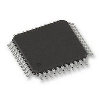
PIC18F45K80-I/PT Microchip Technology, PIC18F45K80-I/PT Datasheet - Page 141

PIC18F45K80-I/PT
Manufacturer Part Number
PIC18F45K80-I/PT
Description
MCU PIC 32KB FLASH 44TQFP
Manufacturer
Microchip Technology
Series
PIC® XLP™ 18Fr
Datasheet
1.PIC18F25K80-ISO.pdf
(628 pages)
Specifications of PIC18F45K80-I/PT
Core Size
8-Bit
Program Memory Size
32KB (16K x 16)
Peripherals
Brown-out Detect/Reset, LVD, POR, PWM, WDT
Core Processor
PIC
Speed
64MHz
Connectivity
ECAN, I²C, LIN, SPI, UART/USART
Number Of I /o
35
Program Memory Type
FLASH
Eeprom Size
1K x 8
Ram Size
3.6K x 8
Voltage - Supply (vcc/vdd)
1.8 V ~ 5.5 V
Data Converters
A/D 11x12b
Oscillator Type
Internal
Operating Temperature
-40°C ~ 85°C
Package / Case
44-TQFP
Controller Family/series
PIC18
Ram Memory Size
4KB
Cpu Speed
16MIPS
No. Of Pwm Channels
5
Embedded Interface Type
I2C, SPI, USART
Processor Series
PIC18F45K80
Core
PIC
Data Bus Width
8 bit
Data Ram Size
1 KB
Interface Type
I2C, SPI, USART
Maximum Clock Frequency
64 MHz
Number Of Programmable I/os
35
Number Of Timers
5
Operating Supply Voltage
1.8 V to 5.5 V
Maximum Operating Temperature
+ 85 C
Mounting Style
SMD/SMT
Lead Free Status / RoHS Status
Lead free / RoHS Compliant
Lead Free Status / RoHS Status
Lead free / RoHS Compliant
Available stocks
Company
Part Number
Manufacturer
Quantity
Price
Company:
Part Number:
PIC18F45K80-I/PT
Manufacturer:
MICROCHIP
Quantity:
1 500
Company:
Part Number:
PIC18F45K80-I/PT
Manufacturer:
PIC
Quantity:
400
Company:
Part Number:
PIC18F45K80-I/PT
Manufacturer:
Microchip Technology
Quantity:
10 000
Part Number:
PIC18F45K80-I/PT
Manufacturer:
MICROCHIP/微芯
Quantity:
20 000
- Current page: 141 of 628
- Download datasheet (6Mb)
7.5
The programming blocks are 32 words or 64 bytes.
Word or byte programming is not supported.
Table writes are used internally to load the holding regis-
ters needed to program the Flash memory. There are
64 holding registers for programming by the table writes.
Since the Table Latch (TABLAT) is only a single byte, the
TBLWT instruction may need to be executed 64 times for
each programming operation. All of the table write oper-
ations will essentially be short writes because only the
holding registers are written. At the end of updating the
64 or 128 holding registers, the EECON1 register must
be written to in order to start the programming operation
with a long write.
The long write is necessary for programming the inter-
nal Flash. Instruction execution is halted while in a long
write cycle. The long write is terminated by the internal
programming timer.
FIGURE 7-5:
7.5.1
The sequence of events for programming an internal
program memory location should be:
1.
2.
3.
4.
5.
6.
7.
8.
2011 Microchip Technology Inc.
TBLPTR = xxxxx0
Read the 64 bytes into RAM.
Update the data values in RAM as necessary.
Load Table Pointer register with the address
being erased.
Execute the row erase procedure.
Load Table Pointer register with the address of
the first byte being written.
Write the 64 bytes into the holding registers with
auto-increment.
Set the EECON1 register for the write operation:
• Set the EEPGD bit to point to program memory
• Clear the CFGS bit to access program memory
• Set the WREN to enable byte writes
Disable the interrupts.
Writing to Flash Program Memory
FLASH PROGRAM MEMORY WRITE
SEQUENCE
Holding Register
8
TABLE WRITES TO FLASH PROGRAM MEMORY
TBLPTR = xxxxx1
Holding Register
8
Preliminary
Program Memory
TBLPTR = xxxxx2
Write Register
TABLAT
PIC18F66K80 FAMILY
The EEPROM on-chip timer controls the write time.
The write/erase voltages are generated by an on-chip
charge pump, rated to operate over the voltage range
of the device.
9.
10. Write 0AAh to EECON2.
11. Set the WR bit. This will begin the write cycle.
12. Re-enable the interrupts.
13. Verify the memory (table read).
An example of the required code is shown in
Example 7-3
Holding Register
Note:
Note:
Write 55h to EECON2.
The CPU will stall for duration of the write for T
(see Parameter D133A).
8
operation.
The default value of the holding registers on
device Resets and after write operations is
FFh. A write of FFh to a holding register
does not modify that byte. This means that
individual bytes of program memory may
be modified, provided that the change does
not attempt to change any bit from a ‘ 0 ’ to a
‘ 1 ’. When modifying individual bytes, it is
not necessary to load all 64 holding
registers
Before setting the WR bit, the Table
Pointer address needs to be within the
intended address range of the 64 bytes in
the holding register.
on the following page.
before
TBLPTR = xxxx3F
executing
DS39977C-page 141
Holding Register
8
a
write
IW
Related parts for PIC18F45K80-I/PT
Image
Part Number
Description
Manufacturer
Datasheet
Request
R

Part Number:
Description:
Manufacturer:
Microchip Technology Inc.
Datasheet:

Part Number:
Description:
Manufacturer:
Microchip Technology Inc.
Datasheet:

Part Number:
Description:
Manufacturer:
Microchip Technology Inc.
Datasheet:

Part Number:
Description:
Manufacturer:
Microchip Technology Inc.
Datasheet:

Part Number:
Description:
Manufacturer:
Microchip Technology Inc.
Datasheet:

Part Number:
Description:
Manufacturer:
Microchip Technology Inc.
Datasheet:

Part Number:
Description:
Manufacturer:
Microchip Technology Inc.
Datasheet:

Part Number:
Description:
Manufacturer:
Microchip Technology Inc.
Datasheet:


