PIC18F45K80-I/PT Microchip Technology, PIC18F45K80-I/PT Datasheet - Page 461
PIC18F45K80-I/PT
Manufacturer Part Number
PIC18F45K80-I/PT
Description
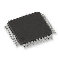
MCU PIC 32KB FLASH 44TQFP
Manufacturer
Microchip Technology
Series
PIC® XLP™ 18Fr
Datasheet
1.PIC18F25K80-ISO.pdf
(628 pages)
Specifications of PIC18F45K80-I/PT
Core Size
8-Bit
Program Memory Size
32KB (16K x 16)
Peripherals
Brown-out Detect/Reset, LVD, POR, PWM, WDT
Core Processor
PIC
Speed
64MHz
Connectivity
ECAN, I²C, LIN, SPI, UART/USART
Number Of I /o
35
Program Memory Type
FLASH
Eeprom Size
1K x 8
Ram Size
3.6K x 8
Voltage - Supply (vcc/vdd)
1.8 V ~ 5.5 V
Data Converters
A/D 11x12b
Oscillator Type
Internal
Operating Temperature
-40°C ~ 85°C
Package / Case
44-TQFP
Controller Family/series
PIC18
Ram Memory Size
4KB
Cpu Speed
16MIPS
No. Of Pwm Channels
5
Embedded Interface Type
I2C, SPI, USART
Processor Series
PIC18F45K80
Core
PIC
Data Bus Width
8 bit
Data Ram Size
1 KB
Interface Type
I2C, SPI, USART
Maximum Clock Frequency
64 MHz
Number Of Programmable I/os
35
Number Of Timers
5
Operating Supply Voltage
1.8 V to 5.5 V
Maximum Operating Temperature
+ 85 C
Mounting Style
SMD/SMT
Lead Free Status / RoHS Status
Lead free / RoHS Compliant
Lead Free Status / RoHS Status
Lead free / RoHS Compliant
Available stocks
Company
Part Number
Manufacturer
Quantity
Price
Company:

Part Number:
PIC18F45K80-I/PT
Manufacturer:
MICROCHIP
Quantity:
1 500
Company:
Part Number:
PIC18F45K80-I/PT
Manufacturer:
PIC
Quantity:
400
Company:
Part Number:
PIC18F45K80-I/PT
Manufacturer:
Microchip Technology
Quantity:
10 000
Part Number:
PIC18F45K80-I/PT
Manufacturer:
MICROCHIP/微芯
Quantity:
20 000


28.0
The PIC18F66K80 family of devices includes several
features intended to maximize reliability and minimize
cost through elimination of external components.
These include:
• Oscillator Selection
• Resets:
• Interrupts
• Watchdog Timer (WDT) and On-chip Regulator
• Fail-Safe Clock Monitor
• Two-Speed Start-up
• Code Protection
• ID Locations
• In-Circuit Serial Programming™
The oscillator can be configured for the application
depending on frequency, power, accuracy and cost. All
of the options are discussed in detail in
“Oscillator Configurations”
A complete discussion of device Resets and interrupts
is available in previous sections of this data sheet.
In addition to their Power-up and Oscillator Start-up
Timers provided for Resets, the PIC18F66K80 family of
devices has a Watchdog Timer, which is either perma-
nently enabled via the Configuration bits or software
controlled (if configured as disabled).
The inclusion of an internal RC oscillator (LF-INTOSC)
also provides the additional benefits of a Fail-Safe
Clock Monitor (FSCM) and Two-Speed Start-up. FSCM
provides for background monitoring of the peripheral
clock and automatic switchover in the event of its fail-
ure. Two-Speed Start-up enables code to be executed
almost immediately on start-up, while the primary clock
source completes its start-up delays.
All of these features are enabled and configured by
setting the appropriate Configuration register bits.
2011 Microchip Technology Inc.
- Power-on Reset (POR)
- Power-up Timer (PWRT)
- Oscillator Start-up Timer (OST)
- Brown-out Reset (BOR)
SPECIAL FEATURES OF THE
CPU
.
Section 3.0
Preliminary
PIC18F66K80 FAMILY
28.1
The Configuration bits can be programmed (read as
‘ 0 ’) or left unprogrammed (read as ‘ 1 ’) to select various
device configurations. These bits are mapped starting
at program memory location, 300000h.
The user will note that address, 300000h, is beyond the
user program memory space. In fact, it belongs to the
configuration memory space (300000h-3FFFFFh),
which can only be accessed using table reads and
table writes.
Software programming the Configuration registers is
done in a manner similar to programming the Flash
memory. The WR bit in the EECON1 register starts a
self-timed write to the Configuration register. In normal
operation mode, a TBLWT instruction with the TBLPTR
pointing to the Configuration register sets up the address
and the data for the Configuration register write. Setting
the WR bit starts a long write to the Configuration
register. The Configuration registers are written a byte at
a time. To write or erase a configuration cell, a TBLWT
instruction can write a ‘ 1 ’ or a ‘ 0 ’ into the cell. For
additional details on Flash programming, refer to
Section 7.5 “Writing to Flash Program Memory”
Configuration Bits
DS39977C-page 461
.
Related parts for PIC18F45K80-I/PT
Image
Part Number
Description
Manufacturer
Datasheet
Request
R

Part Number:
Description:
Manufacturer:
Microchip Technology Inc.
Datasheet:
Part Number:
Description:
Manufacturer:
Microchip Technology Inc.
Datasheet:
Part Number:
Description:
Manufacturer:
Microchip Technology Inc.
Datasheet:
Part Number:
Description:
Manufacturer:
Microchip Technology Inc.
Datasheet:
Part Number:
Description:
Manufacturer:
Microchip Technology Inc.
Datasheet:
Part Number:
Description:
Manufacturer:
Microchip Technology Inc.
Datasheet:
Part Number:
Description:
Manufacturer:
Microchip Technology Inc.
Datasheet:
Part Number:
Description:
Manufacturer:
Microchip Technology Inc.
Datasheet: