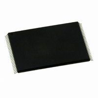
JS28F512P33TFA NUMONYX, JS28F512P33TFA Datasheet - Page 19

JS28F512P33TFA
Manufacturer Part Number
JS28F512P33TFA
Description
IC FLASH 512MBIT P33 65NM 56TSOP
Manufacturer
NUMONYX
Series
Axcell™r
Datasheet
1.JS28F00AP33TF.pdf
(86 pages)
Specifications of JS28F512P33TFA
Format - Memory
FLASH
Memory Type
FLASH
Memory Size
512M (32Mx16)
Speed
105ns
Interface
Parallel
Voltage - Supply
2.3 V ~ 3.6 V
Operating Temperature
-40°C ~ 85°C
Package / Case
56-TSOP
Cell Type
NOR
Density
512Mb
Access Time (max)
105/17ns
Interface Type
Parallel/Serial
Boot Type
Top
Address Bus
25b
Operating Supply Voltage (typ)
2.5/3.3V
Operating Temp Range
-40C to 85C
Package Type
TSOP
Program/erase Volt (typ)
8.5 to 9.5V
Sync/async
Async/Sync
Operating Temperature Classification
Industrial
Operating Supply Voltage (min)
2.3V
Operating Supply Voltage (max)
3.6V
Word Size
16b
Number Of Words
32M
Supply Current
31mA
Mounting
Surface Mount
Pin Count
56
Lead Free Status / RoHS Status
Lead free / RoHS Compliant
Other names
904399
904399
JS28F512P33TF 904399
904399
JS28F512P33TF 904399
Available stocks
Company
Part Number
Manufacturer
Quantity
Price
Company:
Part Number:
JS28F512P33TFA
Manufacturer:
QUALCOMM
Quantity:
920
Part Number:
JS28F512P33TFA
Manufacturer:
INTEL/英特尔
Quantity:
20 000
P33-65nm
6.0
6.1
Table 6:
Datasheet
21
Mode
Erase
Write
Read
Command Codes and Definitions (Sheet 1 of 2)
Command Set
Device Command Codes
The flash Command User Interface (CUI) provides control of all read, write, and erase
operations. The on-chip WSM manages all block-erase and word-program algorithms.
Device commands are written to the CUI to control all flash memory device operations.
The CUI does not occupy an addressable memory location; it is the mechanism through
which the flash device is controlled.
descriptions.
Code
0xD0
0xD0
0xD0
0x70
0x90
0x98
0x50
0x40
0xE8
0x80
0x20
0xFF
Read Array
Read Status
Register
Read Device ID
or Read
Configuration
Register(RCR)
Read CFI
Clear Status
Register
Word Program
Setup
Buffered Program
Buffered Program
Confirm
BEFP Setup
BEFP Confirm
Block Erase Setup
Block Erase Confirm
Device Mode
Places the device in Read Array mode. Array data is output on DQ[15:0].
Places the device in Read Status Register mode. The device enters this mode
after a program or erase command is issued. SR data is output on DQ[7:0].
Places device in Read Device Identifier mode. Subsequent reads output
manufacturer/device codes, Read Configuration Register data, Block Lock
status, or OTP Register data on DQ[15:0].
Places the device in Read Query mode. Subsequent reads output Common
Flash Interface information on DQ[7:0].
The WSM can only set SR error bits. The Clear Status Register command is
used to clear the SR error bits.
First cycle of a 2-cycle programming command; prepares the CUI for a write
operation. On the next write cycle, the address and data are latched and the
WSM executes the programming algorithm at the addressed location. During
program operations, the device responds only to Read Status Register and
Program Suspend commands. CE# or OE# must be toggled to update the
Status Register in asynchronous read. CE# or ADV# must be toggled to
update the SR Data for synchronous Non-array reads. The Read Array
command must be issued to read array data after programming has finished.
This command loads a variable number of words up to the buffer size of 512
words onto the program buffer.
The confirm command is issued after the data streaming for writing into the
buffer is done. This instructs the WSM to perform the Buffered Program
algorithm, writing the data from the buffer to the flash memory array.
First cycle of a 2-cycle command; initiates the BEFP mode. The CUI then
waits for the BEFP Confirm command, 0xD0, that initiates the BEFP
algorithm. All other commands are ignored when BEFP mode begins.
If the previous command was BEFP Setup (0x80), the CUI latches the
address and data, and prepares the device for BEFP mode.
First cycle of a 2-cycle command; prepares the CUI for a block-erase
operation. The WSM performs the erase algorithm on the block addressed by
the Erase Confirm command. If the next command is not the Erase Confirm
(0xD0) command, the CUI sets Status Register bits SR[5,4], and places the
device in Read Status Register mode.
If the first command was Block Erase Setup (0x20), the CUI latches the
address and data, and the WSM erases the addressed block. During block-
erase operations, the device responds only to Read Status Register and Erase
Suspend commands. CE# or OE# must be toggled to update the Status
Register in asynchronous read. CE# or ADV# must be toggled to update the
SR Data for synchronous Non-array reads.
Table 6
shows valid device command codes and
Description
Order Number:208043-05
Apr 2010


