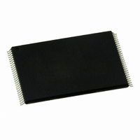
JS28F512P33TFA NUMONYX, JS28F512P33TFA Datasheet - Page 46

JS28F512P33TFA
Manufacturer Part Number
JS28F512P33TFA
Description
IC FLASH 512MBIT P33 65NM 56TSOP
Manufacturer
NUMONYX
Series
Axcell™r
Datasheet
1.JS28F00AP33TF.pdf
(86 pages)
Specifications of JS28F512P33TFA
Format - Memory
FLASH
Memory Type
FLASH
Memory Size
512M (32Mx16)
Speed
105ns
Interface
Parallel
Voltage - Supply
2.3 V ~ 3.6 V
Operating Temperature
-40°C ~ 85°C
Package / Case
56-TSOP
Cell Type
NOR
Density
512Mb
Access Time (max)
105/17ns
Interface Type
Parallel/Serial
Boot Type
Top
Address Bus
25b
Operating Supply Voltage (typ)
2.5/3.3V
Operating Temp Range
-40C to 85C
Package Type
TSOP
Program/erase Volt (typ)
8.5 to 9.5V
Sync/async
Async/Sync
Operating Temperature Classification
Industrial
Operating Supply Voltage (min)
2.3V
Operating Supply Voltage (max)
3.6V
Word Size
16b
Number Of Words
32M
Supply Current
31mA
Mounting
Surface Mount
Pin Count
56
Lead Free Status / RoHS Status
Lead free / RoHS Compliant
Other names
904399
904399
JS28F512P33TF 904399
904399
JS28F512P33TF 904399
Available stocks
Company
Part Number
Manufacturer
Quantity
Price
Company:
Part Number:
JS28F512P33TFA
Manufacturer:
QUALCOMM
Quantity:
920
Part Number:
JS28F512P33TFA
Manufacturer:
INTEL/英特尔
Quantity:
20 000
13.0
13.1
Warning:
Table 19: Absolute Maximum Ratings
13.2
Note:
Table 20: Operating Conditions
Datasheet
48
Temperature under bias
Storage temperature
Voltage on any signal (except VCC, VPP and VCCQ)
VPP voltage
VCC voltage
VCCQ voltage
Output short circuit current
Notes:
1.
2.
3.
4.
Notes:
1.
2.
Symbol
Cycles
VCCQ
Block
Erase
V
VCC
V
t
T
PPH
PPH
PPL
C
Voltages shown are specified with respect to V
VCC, VCCQ, and VPP. During transitions, this level may undershoot to –2.0V for periods less than 20ns. Maximum DC
voltage on VCC is VCC + 0.5V, which, during transitions, may overshoot to VCC + 2.0V for periods less than 20ns.
Maximum DC voltage on input/output signals and VCCQ is VCCQ + 0.5V, which, during transitions, may overshoot to
VCCQ + 2.0V for periods less than 20ns.
Maximum DC voltage on VPP may overshoot to +11.5V for periods less than 20ns.
Program/erase voltage is typically 2.3V – 3.6V. 9.0V can be applied for 80 hours maximum total, to any blocks for
1000 cycles maximum. 9.0V program/erase voltage may reduce block cycling capability.
Output shorted for no more than one second. No more than one output shorted at a time.
T
In typical operation VPP program voltage is V
C
= Case Temperature.
Operating Temperature
VCC Supply Voltage
I/O Supply Voltage
V
Buffered Enhanced Factory Programming V
Maximum V
Array Blocks
PP
Voltage Supply (Logic Level)
Maximum Ratings and Operating Conditions
Absolute Maximum Ratings
Stressing the device beyond the Absolute Maximum Ratings may cause permanent
damage. These are stress ratings only.
Operating Conditions
Operation beyond the Operating Conditions is not recommended and extended
exposure beyond the Operating Conditions may affect device reliability.
PP
Hours
Parameter
Parameter
PPL
SS
PP
CMOS inputs
TTL inputs
VPP = V
VPP = V
VPP = V
.
. Minimum DC voltage is –0.5V on input/output signals and –0.2V on
PPH
PPL
PPH
100,000
Min
–40
2.3
2.3
2.4
1.5
8.5
-
-
Maximum Rating
–65°C to +125°C
–0.2V to +10.0V
–40°C to +85°C
–0.5V to +4.1V
–0.2V to +4.1V
–0.2V to +4.1V
1,000
Max
+85
3.6
3.6
3.6
3.6
9.5
80
-
100mA
Cycles
Hours
Order Number: 208043-05
Unit
°C
V
Notes
1, 3
2
-
Notes
P33-65nm
1,2,3
1
1
1
4
Apr 2010
-
-


