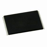
JS28F512P33TFA NUMONYX, JS28F512P33TFA Datasheet - Page 42

JS28F512P33TFA
Manufacturer Part Number
JS28F512P33TFA
Description
IC FLASH 512MBIT P33 65NM 56TSOP
Manufacturer
NUMONYX
Series
Axcell™r
Datasheet
1.JS28F00AP33TF.pdf
(86 pages)
Specifications of JS28F512P33TFA
Format - Memory
FLASH
Memory Type
FLASH
Memory Size
512M (32Mx16)
Speed
105ns
Interface
Parallel
Voltage - Supply
2.3 V ~ 3.6 V
Operating Temperature
-40°C ~ 85°C
Package / Case
56-TSOP
Cell Type
NOR
Density
512Mb
Access Time (max)
105/17ns
Interface Type
Parallel/Serial
Boot Type
Top
Address Bus
25b
Operating Supply Voltage (typ)
2.5/3.3V
Operating Temp Range
-40C to 85C
Package Type
TSOP
Program/erase Volt (typ)
8.5 to 9.5V
Sync/async
Async/Sync
Operating Temperature Classification
Industrial
Operating Supply Voltage (min)
2.3V
Operating Supply Voltage (max)
3.6V
Word Size
16b
Number Of Words
32M
Supply Current
31mA
Mounting
Surface Mount
Pin Count
56
Lead Free Status / RoHS Status
Lead free / RoHS Compliant
Other names
904399
904399
JS28F512P33TF 904399
904399
JS28F512P33TF 904399
Available stocks
Company
Part Number
Manufacturer
Quantity
Price
Company:
Part Number:
JS28F512P33TFA
Manufacturer:
QUALCOMM
Quantity:
920
Part Number:
JS28F512P33TFA
Manufacturer:
INTEL/英特尔
Quantity:
20 000
Figure 13: OTP Register Map
11.3.1
11.3.2
Datasheet
44
Reading the OTP Registers
The OTP Registers can be read from OTP-RA address. To read the OTP Register, first
issue the Read Device Identifier command at OTP-RA address to place the device in the
Read Device Identifier state (see
page
register to be read.
address offsets of the OTP Registers and Lock Registers. OTP Register and Lock
Register data is read 16 bits at a time.
Programming the OTP Registers
To program an OTP Registers, first issue the Program OTP Register command at the
device base address plus the offset of the desired OTP Register location (See
“OTP Register Map” on page
OTP Register address. See
22). Next, perform a read operation using the address offset corresponding to the
0x109
0x102
0x8A
0x91
0x89
0x88
0x85
0x84
0x81
0x80
15 14 13 12 11 10 9
15 14 13 12 11 10 9
Table 8, “Device Identifier Information” on page 24
128-bit OTP Register 16
(Factory-Programmed)
128-bit OTP Register 1
(User-Programmable)
(User-Programmable)
(User-Programmable)
128-Bit OTP Register 0
Section 6.2, “Device Command Bus Cycles” on page
Lock Register 1
64-bit Segment
64-bit Segment
44). Next, write the desired OTP Register data to the same
Lock Register 0
8
8
7
7
Section 6.2, “Device Command Bus Cycles” on
6
6
5
5
4
4
3
3
2
2
1
1
0
0
Order Number: 208043-05
shows the
Figure 13,
P33-65nm
22.
Apr 2010


