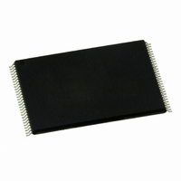
JS28F512P33TFA NUMONYX, JS28F512P33TFA Datasheet - Page 5

JS28F512P33TFA
Manufacturer Part Number
JS28F512P33TFA
Description
IC FLASH 512MBIT P33 65NM 56TSOP
Manufacturer
NUMONYX
Series
Axcell™r
Datasheet
1.JS28F00AP33TF.pdf
(86 pages)
Specifications of JS28F512P33TFA
Format - Memory
FLASH
Memory Type
FLASH
Memory Size
512M (32Mx16)
Speed
105ns
Interface
Parallel
Voltage - Supply
2.3 V ~ 3.6 V
Operating Temperature
-40°C ~ 85°C
Package / Case
56-TSOP
Cell Type
NOR
Density
512Mb
Access Time (max)
105/17ns
Interface Type
Parallel/Serial
Boot Type
Top
Address Bus
25b
Operating Supply Voltage (typ)
2.5/3.3V
Operating Temp Range
-40C to 85C
Package Type
TSOP
Program/erase Volt (typ)
8.5 to 9.5V
Sync/async
Async/Sync
Operating Temperature Classification
Industrial
Operating Supply Voltage (min)
2.3V
Operating Supply Voltage (max)
3.6V
Word Size
16b
Number Of Words
32M
Supply Current
31mA
Mounting
Surface Mount
Pin Count
56
Lead Free Status / RoHS Status
Lead free / RoHS Compliant
Other names
904399
904399
JS28F512P33TF 904399
904399
JS28F512P33TF 904399
Available stocks
Company
Part Number
Manufacturer
Quantity
Price
Company:
Part Number:
JS28F512P33TFA
Manufacturer:
QUALCOMM
Quantity:
920
Part Number:
JS28F512P33TFA
Manufacturer:
INTEL/英特ه°”
Quantity:
20 000
P33-65nm
1.0
1.1
1.2
Datasheet
7
Functional Description
Introduction
This document provides information about the Numonyx
memory and describes its features, operations, and specifications.
P33-65nm is the latest generation of Numonyx
embedded flash market segment, offered in 64-Mbit up through 2-Gbit. This document
covers specifically 512-Mbit, 1-Gbit, 2-Gbit product information. Benefits include more
density in less space, high-speed interface NOR device on TSOP package, and support
for code and data storage. Features include high-performance synchronous-burst read
mode, dramatical improvement in buffer program time through larger buffer size, fast
asynchronous access times, low power, flexible security options, and two industry-
standard package choices.
P33-65nm is manufactured using Numonyx
Overview
The P33-65nm device provides high performance on a 16-bit data bus. Individually
erasable memory blocks are sized for optimum code and data storage. Upon initial
power-up or return from reset, the device defaults to asynchronous page-mode read.
Configuring the RCR(Read Configuration Register) enables synchronous burst-mode
reads. In synchronous burst mode, output data is synchronized with a user-supplied
clock signal. A WAIT signal provides an easy CPU-to-flash memory synchronization.
In addition to the enhanced architecture and interface, the device incorporates
technology that enables fast buffer program and erase operations. The device features
a 512-word buffer to enable optimum programming performance, which can improve
system programming throughput time significantly to 1.46MByte/s.
Designed for low-voltage systems, P33-65nm device supports read operations with VCC
at 3.0V, and erase and program operations with VPP at 3.0V or 9.0V. Buffered
Enhanced Factory Programming provides the fastest flash array programming
performance with VPP at 9.0V, which increases factory throughput. With VPP at 3.0V,
VCC and VPP can be tied together for a simple, ultra low power design. In addition to
voltage flexibility, a dedicated VPP connection provides complete data protection when
VPP ≤ V
The Command User Interface is the interface between the system processor and all
internal operations of the device. An internal Write State Machine automatically
executes the algorithms and timings necessary for block erase and program. A Status
Register indicates erase or program completion and any errors that may have occurred.
A device command sequence invokes program and erase automation. Each erase
operation erases one block. The Erase Suspend feature allows system software to
pause an erase cycle to read or program data in another block. Program Suspend
allows system software to pause programming to read other locations.
The P33-65nm OTP Register allows unique flash device identification that can be used
to increase system security. The individual Block Lock feature provides zero-latency
block locking and unlocking. The P33-65nm device adds enhanced protection via
Password Access; this new feature allows write and/or read access protection of user-
defined blocks. In addition, the P33-65nm device also has backward compatible One-
Time Programmable (OTP) permanent block locking security feature.
PPLK
.
®
65nm process technology.
®
Axcell
TM
®
P33 Flash memory to the
Axcell
TM
Order Number:208043-05
P33-65nm Flash
Apr 2010


