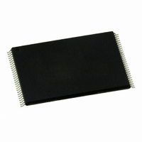
JS28F512P33TFA NUMONYX, JS28F512P33TFA Datasheet - Page 6

JS28F512P33TFA
Manufacturer Part Number
JS28F512P33TFA
Description
IC FLASH 512MBIT P33 65NM 56TSOP
Manufacturer
NUMONYX
Series
Axcell™r
Datasheet
1.JS28F00AP33TF.pdf
(86 pages)
Specifications of JS28F512P33TFA
Format - Memory
FLASH
Memory Type
FLASH
Memory Size
512M (32Mx16)
Speed
105ns
Interface
Parallel
Voltage - Supply
2.3 V ~ 3.6 V
Operating Temperature
-40°C ~ 85°C
Package / Case
56-TSOP
Cell Type
NOR
Density
512Mb
Access Time (max)
105/17ns
Interface Type
Parallel/Serial
Boot Type
Top
Address Bus
25b
Operating Supply Voltage (typ)
2.5/3.3V
Operating Temp Range
-40C to 85C
Package Type
TSOP
Program/erase Volt (typ)
8.5 to 9.5V
Sync/async
Async/Sync
Operating Temperature Classification
Industrial
Operating Supply Voltage (min)
2.3V
Operating Supply Voltage (max)
3.6V
Word Size
16b
Number Of Words
32M
Supply Current
31mA
Mounting
Surface Mount
Pin Count
56
Lead Free Status / RoHS Status
Lead free / RoHS Compliant
Other names
904399
904399
JS28F512P33TF 904399
904399
JS28F512P33TF 904399
Available stocks
Company
Part Number
Manufacturer
Quantity
Price
Company:
Part Number:
JS28F512P33TFA
Manufacturer:
QUALCOMM
Quantity:
920
Part Number:
JS28F512P33TFA
Manufacturer:
INTEL/英特ه°”
Quantity:
20 000
1.3
Table 1:
Datasheet
8
Flash Die Virtual Chip Enable Truth Table for 2-Gbit (1-Gbit/1-Gbit) Devices
Virtual Chip Enable Description (2-Gbit)
The P33-65nm device employs a Virtual Chip Enable to combine two 1-Gbit dies with a
common chip enable, CE#, for Easy BGA, Address A27 is then used to select between
the die pair with CE# asserted. When chip enable is asserted and A27 is low (
lower die is selected; when chip enable is asserted and A27 is high (
is selected.
Die Selected
Lower Die
Upper Die
CE#
L
L
Order Number: 208043-05
V
IH
), the upper die
A27
H
L
V
P33-65nm
IL
Apr 2010
), the


