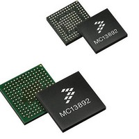
MC13892JVL Freescale Semiconductor, MC13892JVL Datasheet - Page 105

MC13892JVL
Manufacturer Part Number
MC13892JVL
Description
IC PMU I.MX51/37/35/27 186MAPBGA
Manufacturer
Freescale Semiconductor
Datasheets
1.MC13892AJVLR2.pdf
(156 pages)
2.MC13892AJVLR2.pdf
(2 pages)
3.MC13892AJVLR2.pdf
(16 pages)
4.MC13892JVL.pdf
(161 pages)
Specifications of MC13892JVL
Applications
Battery Management, Display (LED Drivers), Handheld/Mobile Devices, Power Supply
Operating Temperature
-40°C ~ 85°C
Mounting Type
Surface Mount
Package / Case
186-LFBGA
Output Current
65 mA
Output Voltage
1.5 V
Operating Temperature (max)
85C
Operating Temperature (min)
-40C
Mounting
Surface Mount
Package Type
BGA
Case Length
12mm
Screening Level
Industrial
Lead Free Status / RoHS Status
Lead free / RoHS Compliant
Current - Supply
-
Voltage - Supply
-
Lead Free Status / Rohs Status
Lead free / RoHS Compliant
Available stocks
Company
Part Number
Manufacturer
Quantity
Price
Company:
Part Number:
MC13892JVL
Manufacturer:
DALSA
Quantity:
4
Company:
Part Number:
MC13892JVL
Manufacturer:
Freescale Semiconductor
Quantity:
10 000
Part Number:
MC13892JVL
Manufacturer:
FREESCALE
Quantity:
20 000
Company:
Part Number:
MC13892JVLR2
Manufacturer:
Freescale Semiconductor
Quantity:
10 000
ADC conversion ADCDONEI, and one for the ADCBIS conversion ADCBISDONEI. These interrupts will go high after the
conversion, and can be masked.
conversion of the first request, an ADTRIG trigger event of the other request is ignored, if for the other request the TRIGMASK
bit was set to 1. When this bit is set to 0, the other request ADTRIG trigger event is memorized, and the conversion will take place
directly after the conversions of the first request are finished.
conversion has to be lined up to a periodically ADTRIG initiated conversion. In case of ASC initiated conversions, the TRIGMASK
bit is of no influence.
by setting the ADONESHOT bit to a one. In that case, only at the first following conversion, an ADTRIG trigger event is accepted.
ASC events are not affected by this setting. Before performing a new single shot conversion, the ADONESHOT bit first needs to
be cleared. Note that this bit is available for each of the conversion requests 'ADC' or 'ADC BIS', so can be set independently.
TRIGMASK setting. If both conversion requests have identical TRIGMASK settings, priority is given to the 'ADC' conversion over
the 'ADC BIS' conversion. Note that the ADONESHOT is also taken into account.
transition on the ADTRIG pin. The ADC completely ignores either ADTRIG or ASC pulses while ADEN is low. When reading
conversion results, it is preferable to make ADEN = 0.
Analog Integrated Circuit Device Data
Freescale Semiconductor
There are two interrupts available to inform the processor when the ADC has finished its conversions, one for the standard
When two requests are queued, the request for which the trigger event occurs the first will be converted the first. During the
The following diagram shows the influence of the TRIGMASK bit. The TRIGMASK bit is particularly of use when an ADC
To avoid results of previous conversions getting overwritten by a periodical ADTRIG signal, a single shot function is enabled
It is possible to queue two ADTRIG triggered conversions. Both conversions will be executed with a priority based on the
To avoid that the ADTRIG input inadvertently triggers a conversion, the ADTRIGIGN bit can be set which will ignore any
Location
Location
Location
Location
Location
43
44
45
46
47
Register ADC0
Register ADC1
ADC Control
ADC Control
ADC Control
ADC Result
ADC Result
Register 0
Register 1
Register 2
R/W
R/W
R/W
R/W
R/W
Bi t
Bi t
Bi t
Bi t
Bi t
Figure 28. ADC Register Set for ADC BIS Access
8 Bit Address Header
Figure 29. TRIGMASK Functional Diagram
Address
Address
Address
Address
Address
Bits
Bits
Bits
Bits
Bits
Nul l
Nul l
Nul l
Nul l
Nul l
Bi t
Bi t
Bi t
Bi t
Bi t
ADC
BIS0
ADC
BIS1
ADC
BIS2
ADC BIS Result
ADC Result
24 B it Data
ADC Control
ADC Control
ADC Control
Bits
Bits
Bits
Bits
Bits
FUNCTIONAL DEVICE OPERATION
ADC SUBSYSTEM
13892
105


