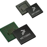
MC13892JVL Freescale Semiconductor, MC13892JVL Datasheet - Page 8

MC13892JVL
Manufacturer Part Number
MC13892JVL
Description
IC PMU I.MX51/37/35/27 186MAPBGA
Manufacturer
Freescale Semiconductor
Datasheets
1.MC13892AJVLR2.pdf
(156 pages)
2.MC13892AJVLR2.pdf
(2 pages)
3.MC13892AJVLR2.pdf
(16 pages)
4.MC13892JVL.pdf
(161 pages)
Specifications of MC13892JVL
Applications
Battery Management, Display (LED Drivers), Handheld/Mobile Devices, Power Supply
Operating Temperature
-40°C ~ 85°C
Mounting Type
Surface Mount
Package / Case
186-LFBGA
Output Current
65 mA
Output Voltage
1.5 V
Operating Temperature (max)
85C
Operating Temperature (min)
-40C
Mounting
Surface Mount
Package Type
BGA
Case Length
12mm
Screening Level
Industrial
Lead Free Status / RoHS Status
Lead free / RoHS Compliant
Current - Supply
-
Voltage - Supply
-
Lead Free Status / Rohs Status
Lead free / RoHS Compliant
Available stocks
Company
Part Number
Manufacturer
Quantity
Price
Company:
Part Number:
MC13892JVL
Manufacturer:
DALSA
Quantity:
4
Company:
Part Number:
MC13892JVL
Manufacturer:
Freescale Semiconductor
Quantity:
10 000
Part Number:
MC13892JVL
Manufacturer:
FREESCALE
Quantity:
20 000
Company:
Part Number:
MC13892JVLR2
Manufacturer:
Freescale Semiconductor
Quantity:
10 000
PIN CONNECTIONS
Table 2. 13892 Pin Definitions (continued)
8
13892
Pin Number
13982VK
7x7 mm
A functional description of each pin can be found in the Functional Pin Description section beginning on
on the
G10
G12
G13
F10
F11
F12
F13
G1
G2
G4
G5
G6
G7
G8
G9
H1
H2
H4
H5
H6
H7
H8
H9
F7
F8
F9
E7, E8, E9, E10,
F7, F8, F9, F10,
G4, G5, G6, G7,
K8, K10, L4, L5,
Pin Number on
H3, H5, H6, H7,
J8, J9, J10, K4,
P5, P7, P8, P9,
G9, G10, G11,
H9, H10, H12,
the 13982VL
12x12 mm
K5, K6, K7
F4, F5, F6
J5, J6, J7
H13, H14
L6, L10
H1, H2
C13
E12
E14
C14
D14
P10
F13
F14
F12
F11
G8
F1
F3
E2
H8
P2
N4
J3
L3
RESETBMCU
GNDREG2
GNDREG3
GNDSUB2
GNDSUB3
GNDSUB4
GNDSUB5
GNDSUB6
GNDSUB7
GNDSUB8
GNDSUB9
GNDCTRL
Pin Name
SW1OUT
SW3OUT
RESETB
GNDSPI
VINUSB
SW4FB
PUMS1
SW1IN
SW3IN
GPO3
GPO2
GPO4
MISO
WDI
Rating
3.6
3.6
3.6
5.5
5.5
7.5
3.6
3.6
3.6
3.6
5.5
5.5
3.6
(V)
-
-
-
-
-
-
-
-
-
-
-
-
-
Pin Function
Ground
Ground
Ground
Ground
Ground
Ground
Ground
Ground
Ground
Ground
Ground
Ground
Output
Output
Output
Output
Output
Output
Output
Power
Input
Input
Input
Input
Input
I/O
Power Up Mode Select
Logic Control Ground
Switcher 4 Feedback
Regulator 2 Ground
Master In Slave Out
Regulator 3 Ground
VUSB Supply Input
Switcher 1 Output
Switcher 3 Output
General Purpose
General Purpose
General Purpose
Peripheral Reset
Switcher 1 Input
Switcher 3 Input
Watchdog Input
Formal Name
MCU Reset
SPI Ground
Ground 2
Ground 3
Ground 4
Ground 5
Ground 6
Ground 7
Ground 8
Ground 9
Output 3
Output 2
Output 4
1
Non critical signal ground and thermal heat
sink
Non critical signal ground and thermal heat
sink
General purpose output 3
General purpose output 2
Reset output for processor
Reset output for peripherals
Switcher 1 output
Switcher 3 output
Input option for UVUSB; tie to SWBST at top
level
Switcher 4 feedback
Ground for regulators 2
Non critical signal ground and thermal heat
sink
Non critical signal ground and thermal heat
sink
Non critical signal ground and thermal heat
sink
Power up mode supply setting 1
Watchdog input
General purpose output 4
Switcher 3 input
Primary SPI read output
Ground for SPI interface
Ground for regulators 3
Non critical signal ground and thermal heat
sink
Non critical signal ground and thermal heat
sink
Non critical signal ground and thermal heat
sink
Ground for control logic
Input voltage for switcher 1
Analog Integrated Circuit Device Data
Freescale Semiconductor
Definition
page
32.


