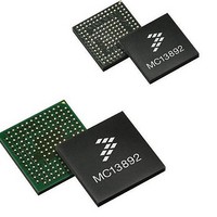
MC13892JVL Freescale Semiconductor, MC13892JVL Datasheet - Page 51

MC13892JVL
Manufacturer Part Number
MC13892JVL
Description
IC PMU I.MX51/37/35/27 186MAPBGA
Manufacturer
Freescale Semiconductor
Datasheets
1.MC13892AJVLR2.pdf
(156 pages)
2.MC13892AJVLR2.pdf
(2 pages)
3.MC13892AJVLR2.pdf
(16 pages)
4.MC13892JVL.pdf
(161 pages)
Specifications of MC13892JVL
Applications
Battery Management, Display (LED Drivers), Handheld/Mobile Devices, Power Supply
Operating Temperature
-40°C ~ 85°C
Mounting Type
Surface Mount
Package / Case
186-LFBGA
Output Current
65 mA
Output Voltage
1.5 V
Operating Temperature (max)
85C
Operating Temperature (min)
-40C
Mounting
Surface Mount
Package Type
BGA
Case Length
12mm
Screening Level
Industrial
Lead Free Status / RoHS Status
Lead free / RoHS Compliant
Current - Supply
-
Voltage - Supply
-
Lead Free Status / Rohs Status
Lead free / RoHS Compliant
Available stocks
Company
Part Number
Manufacturer
Quantity
Price
Company:
Part Number:
MC13892JVL
Manufacturer:
DALSA
Quantity:
4
Company:
Part Number:
MC13892JVL
Manufacturer:
Freescale Semiconductor
Quantity:
10 000
Part Number:
MC13892JVL
Manufacturer:
FREESCALE
Quantity:
20 000
Company:
Part Number:
MC13892JVLR2
Manufacturer:
Freescale Semiconductor
Quantity:
10 000
OSCILLATOR APPLICATION GUIDELINES
of the amplifier and even the drive level to the crystal. (Changing the drive level to the crystal may change the aging rate, jitter,
and even the frequency at a given load capacitance.) The traces should be kept as short as possible to minimize the leakage,
and good PCB manufacturing processes should be maintained.
short as possible with minimal coupling to other signals. The signal ground for the RTC is to be connected to GNDRTC, and via
a single connection, GNDRTC to the system ground. The CLK32K and CLK32KMCU square wave outputs must be kept away
from the crystal / load capacitor leads, as the sharp edges can couple into the circuit and lead to excessive jitter. The crystal /
load capacitance leads and the RTC Ground must form a minimal loop area.
a given manufacturer. If a different crystal is considered, it must be fully characterized with the MC13892 before it can be
considered.
composed out of the load capacitance, the effective input capacitance at each pin, plus the PCB stray capacitance for each pin.
SRTC SUPPORT
providing a VSRTC voltage to bias the SRTC module of the processor, as well as a CLK32KMCU at the VSRTC output level.
to ensure that the SRTC module always has its reference clock. If DRM = 0, the CLK32KMCU driver will not be maintained in the
Off state. Refer to
internal MEMHOLD PCUT modes.
programmed for such capability. This can be accomplished by connecting an open drain NMOS driver to the PWRON pin of the
MC13892, so that it is in effect a parallel path for the power key. The MC13892 will not be able to discern the turn on event from
a normal power key initiated turn on, but the processor should have the knowledge, since the RTC initiated turn on is generated
locally.
Analog Integrated Circuit Device Data
Freescale Semiconductor
Table 16. Crystal Oscillator Main Characteristics
Operating Voltage
Coin cell Disconnect Threshold
RTC oscillator startup time
XTAL1 Input Level
XTAL1 Input Range
Output Low CLK32K,
CLK32KMCU
Output High
CLK32K Rise and Fall Time
CLD32KMCU Rise and Fall Time
CLK32K and CLK32KMCU
Output Duty Cycle
The guidelines below may prove to be helpful in providing a crystal oscillator that starts reliably and runs with minimal jitter.
PCB leakage: The RTC amplifier is a low current circuit. Therefore, PCB leakage may significantly change the operating point
Layout: The traces from the 13892 to the crystal, load capacitance, and the RTC Ground are sensitive. They must be kept as
Crystal Choice: Generally speaking, crystals are not interchangeable between manufacturers, or even different packages for
Tuning Capacitors: The nominal load capacitance is 9.0 pF, therefore the total capacitance at each node should be 18 pF,
The MC13892 provides support for processors which have an integrated SRTC for Digital Rights Management (DRM), by
When configured for DRM mode (SPI bit DRM = 1), the CLK32MCU driver will be kept enabled through all operational states,
It is also necessary to provide a means for the processor to do an RTC initiated wake-up of the system, if it has been
Parameter
Table 23
for the operating behavior of the CLK32KMCU output in User Off, Memory Hold, User off Wait, and
Oscillator and RTC Block from BP
At LICELL
Upon application of power
External clock source
External clock source
Output sink 100 μA
CLK32K Output source 100 μA
CLK32KMCU Output source 100 μA
CL=50 pF
CLK32KDRV[1:0] = 00 (default)
CLK32KDRV[1:0] = 01
CLK32KDRV[1:0] = 10
CLK32KDRV[1:0] = 11
CL=12 pF
Crystal on XTAL1, XTAL2 pins
Condition
SPIVCC-0.2
VSRTC-0.2
Min
CLOCK GENERATION AND REAL TIME CLOCK
-0.5
1.2
1.8
0.3
45
0
-
-
-
-
-
-
FUNCTIONAL DEVICE OPERATION
High Z
Typ
22
44
22
11
-
-
-
-
-
-
-
-
-
SPIVCC
VSRTC
Max
4.65
2.0
1.0
1.2
0.2
55
-
-
-
-
-
-
Units
V
sec
ns
ns
ns
ns
ns
%
V
V
V
V
V
V
PP
13892
51


