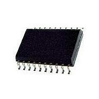
PCA9634PW NXP Semiconductors, PCA9634PW Datasheet - Page 15

PCA9634PW
Manufacturer Part Number
PCA9634PW
Description
IC, LED DRIVER, RGBA, 20-TSSOP
Manufacturer
NXP Semiconductors
Datasheet
1.PCA9634D112.pdf
(38 pages)
Specifications of PCA9634PW
No. Of Outputs
8
Output Current
25mA
Output Voltage
5.5V
Input Voltage
2.3V To 5.5V
Dimming Control Type
PWM
Driver Case Style
TSSOP
Switching Frequency
1MHz
Base Number
9634
Operating
RoHS Compliant
Number Of Segments
16
Low Level Output Current
200 mA
High Level Output Current
50 uA
Operating Supply Voltage
2.3 V to 5.5 V
Maximum Supply Current
10 mA
Maximum Power Dissipation
400 mW
Maximum Operating Temperature
+ 85 C
Mounting Style
SMD/SMT
Package / Case
TSSOP-20
Minimum Operating Temperature
- 40 C
Led Driver Application
RGB Or RGBA LED Drivers, LED Status Information, Displays, Backlights
Rohs Compliant
Yes
Lead Free Status / Rohs Status
Details
Available stocks
Company
Part Number
Manufacturer
Quantity
Price
Company:
Part Number:
PCA9634PW
Manufacturer:
TRINAMIC
Quantity:
1 200
Company:
Part Number:
PCA9634PW
Manufacturer:
NXP Semiconductors
Quantity:
26 963
Part Number:
PCA9634PW
Manufacturer:
NXP/恩智浦
Quantity:
20 000
NXP Semiconductors
PCA9634_6
Product data sheet
7.3.8 ALLCALLADR: LED All Call I
7.4 Active LOW output enable input
Table 12.
Legend: * default value.
The LED All Call I
at the same time (ALLCALL bit in register MODE1 must be equal to 1 (power-up default
state)). This address is programmable through the I
an I
Sub Call.
Only the 7 MSBs representing the All Call I
ALLCALLADR register is a read-only bit (0).
If ALLCALL bit = 0, the device does not acknowledge the address programmed in register
ALLCALLADR.
The active LOW output enable (OE) pin, allows to enable or disable all the LED outputs at
the same time.
Table 13.
The OE pin can be used as a synchronization signal to switch on/off several PCA9634
devices at the same time. This requires an external clock reference that provides blinking
period and the duty cycle.
The OE pin can also be used as an external dimming control signal. The frequency of the
external clock must be high enough not to be seen by the human eye, and the duty cycle
value determines the brightness of the LEDs.
Remark: Do not use OE as an external blinking control signal when internal global
blinking is selected (DMBLNK = 1, MODE2 register) since it will result in an undefined
blinking pattern. Do not use OE as an external dimming control signal when internal global
dimming is selected (DMBLNK = 0, MODE2 register) since it will result in an undefined
dimming pattern.
Address
11h
OUTNE1
0
0
1
1
•
•
2
When a LOW level is applied to OE pin, all the LED outputs are enabled and follow the
output state defined in the LEDOUT register with the polarity defined by INVRT bit
(MODE2 register).
When a HIGH level is applied to OE pin, all the LED outputs are programmed to the
value that is defined by OUTNE[1:0] in the MODE2 register.
C-bus read or write sequence. The register address can also be programmed as a
Register
ALLCALLADR
ALLCALLADR - LED All Call I
description
LED outputs when OE = 1
OUTNE0
0
1
0
1
2
C-bus address allows all the PCA9634s on the bus to be programmed
Rev. 06 — 12 September 2008
Bit
7:1
0
LED outputs
0
1 if OUTDRV = 1, high-impedance if OUTDRV = 0
high-impedance
reserved
Symbol
AC[7:1]
AC[0]
2
C-bus address
2
C-bus address register (address 11h) bit
2
Access Value
R/W
R only
C-bus address are valid. The LSB in
2
C-bus and can be used during either
1110 000*
0*
8-bit Fm+ I
Description
ALLCALL I
address register
reserved
PCA9634
2
© NXP B.V. 2008. All rights reserved.
C-bus LED driver
2
C-bus
15 of 38


