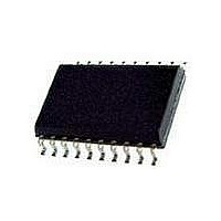
PCA9634PW NXP Semiconductors, PCA9634PW Datasheet - Page 24

PCA9634PW
Manufacturer Part Number
PCA9634PW
Description
IC, LED DRIVER, RGBA, 20-TSSOP
Manufacturer
NXP Semiconductors
Datasheet
1.PCA9634D112.pdf
(38 pages)
Specifications of PCA9634PW
No. Of Outputs
8
Output Current
25mA
Output Voltage
5.5V
Input Voltage
2.3V To 5.5V
Dimming Control Type
PWM
Driver Case Style
TSSOP
Switching Frequency
1MHz
Base Number
9634
Operating
RoHS Compliant
Number Of Segments
16
Low Level Output Current
200 mA
High Level Output Current
50 uA
Operating Supply Voltage
2.3 V to 5.5 V
Maximum Supply Current
10 mA
Maximum Power Dissipation
400 mW
Maximum Operating Temperature
+ 85 C
Mounting Style
SMD/SMT
Package / Case
TSSOP-20
Minimum Operating Temperature
- 40 C
Led Driver Application
RGB Or RGBA LED Drivers, LED Status Information, Displays, Backlights
Rohs Compliant
Yes
Lead Free Status / Rohs Status
Details
Available stocks
Company
Part Number
Manufacturer
Quantity
Price
Company:
Part Number:
PCA9634PW
Manufacturer:
TRINAMIC
Quantity:
1 200
Company:
Part Number:
PCA9634PW
Manufacturer:
NXP Semiconductors
Quantity:
26 963
Part Number:
PCA9634PW
Manufacturer:
NXP/恩智浦
Quantity:
20 000
NXP Semiconductors
10. Application design-in information
PCA9634_6
Product data sheet
Fig 18. Typical application
(1) OE requires pull-up resistor if control signal from the master is open-drain.
I
All of the 8 LEDn outputs configurable as either open-drain or totem pole. Mixing of configurations is not possible.
2
C-bus address = 0010 101X.
I
2
C-BUS/SMBus
MASTER
V
DD
= 2.5 V, 3.3 V or 5.0 V
SDA
SCL
Question 1: What kind of edge rate control is there on the outputs?
Question 2: Is ground bounce possible?
OE
•
•
The typical edge rates depend on the output configuration, supply voltage, and the
applied load. The outputs can be configured as either open-drain NMOS or
totem-pole outputs. If the customer is using the part to directly drive LEDs, they
should be using it in an open-drain NMOS, if they are concerned about the maximum
ISS and ground bounce. The edge rate control was designed primarily to slow down
the turn-on of the output device; it turns off rather quickly (~1.5 ns). In simulation, the
typical turn-on time for the open-drain NMOS was ~14 ns (V
R
Ground bounce is a possibility, especially if all 16 outputs are changed at full current
(25 mA each). There is a fair amount of decoupling capacitance on chip (~50 pF),
which is intended to suppress some of the ground bounce. The customer will need to
determine if additional decoupling capacitance externally placed as close as
physically possible to the device is required.
PU
10 k
= 500 ).
10 k
Rev. 06 — 12 September 2008
10 k (1)
SDA
SCL
OE
A0
A1
A2
A3
A4
A5
A6
V
SS
PCA9634
V
DD
002aac137
LED0
LED1
LED2
LED3
LED4
LED5
LED6
LED7
5 V
5 V
8-bit Fm+ I
DD
= 3.6 V; C
PCA9634
2
© NXP B.V. 2008. All rights reserved.
C-bus LED driver
12 V
12 V
L
= 50 pF;
24 of 38


