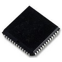
SC16C754BIA68 NXP Semiconductors, SC16C754BIA68 Datasheet - Page 7

SC16C754BIA68
Manufacturer Part Number
SC16C754BIA68
Description
IC, UART, QUAD, 64BYTE FIFO, 16C754
Manufacturer
NXP Semiconductors
Datasheet
1.SC16C754BIA68.pdf
(51 pages)
Specifications of SC16C754BIA68
No. Of Channels
4
Data Rate
5Mbps
Supply Voltage Range
2.25V To 5.5V
Operating Temperature Range
-40°C To +85°C
Digital Ic Case Style
PLCC
No. Of Pins
68
Svhc
No SVHC (18-Jun-2010)
Uart Features
DMA Signalling Capability, Software Selectable Baud Rate Generator
Rohs Compliant
Yes
Lead Free Status / RoHS Status
Lead free / RoHS Compliant
Available stocks
Company
Part Number
Manufacturer
Quantity
Price
Part Number:
SC16C754BIA68
Manufacturer:
NXP/恩智浦
Quantity:
20 000
Company:
Part Number:
SC16C754BIA68,512
Manufacturer:
NXP Semiconductors
Quantity:
10 000
Company:
Part Number:
SC16C754BIA68,518
Manufacturer:
NXP Semiconductors
Quantity:
10 000
Part Number:
SC16C754BIA68,518
Manufacturer:
NXP/恩智浦
Quantity:
20 000
Company:
Part Number:
SC16C754BIA68,529
Manufacturer:
NXP Semiconductors
Quantity:
10 000
NXP Semiconductors
Table 2.
SC16C754B_4
Product data sheet
Symbol
CSA
CSB
CSC
CSD
CTSA
CTSB
CTSC
CTSD
D0 to D7
DSRA
DSRB
DSRC
DSRD
DTRA
DTRB
DTRC
DTRD
GND
INTA
INTB
INTC
INTD
INTSEL
IOR
Pin
LQFP64 LQFP80 PLCC68
7
11
38
42
2
16
33
47
53, 54,
55, 56,
57, 58,
59, 60
1
17
32
48
3
15
34
46
14, 28,
45, 61
6
12
37
43
-
40
Pin description
9
13
49
53
4
18
44
58
68, 69,
70, 71,
72, 73,
74, 75
3
19
43
59
5
17
45
57
16, 36,
56, 76
8
14
48
54
67
51
…continued
16
20
50
54
11
25
45
59
66, 67,
68, 1, 2,
3, 4, 5
10
26
44
60
12
24
46
58
6, 23,
40, 57
15
21
49
55
65
52
Type
I
I
I/O
I
O
I
O
I
I
5 V, 3.3 V and 2.5 V quad UART, 5 Mbit/s (max.) with 64-byte FIFOs
Rev. 04 — 6 October 2008
Description
Chip Select (active LOW). These pins enable data transfers between
the user CPU and the SC16C754B for the channel(s) addressed.
Individual UART sections (A, B, C, D) are addressed by providing a logic
LOW on the respective CSA through CSD pins.
Clear to Send (active LOW). These inputs are associated with individual
UART channels A through D. A logic 0 (LOW) on the CTS pins indicates
the modem or data set is ready to accept transmit data from the
SC16C754B. Status can be tested by reading MSR[4]. These pins only
affect the transmit and receive operations when auto-CTS function is
enabled via the Enhanced Feature Register EFR[7] for hardware flow
control operation.
Data bus (bidirectional). These pins are the 8-bit, 3-state data bus for
transferring information to or from the controlling CPU. D0 is the least
significant bit and the first data bit in a transmit or receive serial data
stream.
Data Set Ready (active LOW). These inputs are associated with
individual UART channels A through D. A logic 0 (LOW) on these pins
indicates the modem or data set is powered-on and is ready for data
exchange with the UART. The state of these inputs is reflected in the
Modem Status Register (MSR).
Data Terminal Ready (active LOW). These outputs are associated with
individual UART channels A through D. A logic 0 (LOW) on these pins
indicates that the SC16C754B is powered-on and ready. These pins can
be controlled via the Modem Control Register (MCR). Writing a logic 1 to
MCR[0] will set the DTR output to logic 0 (LOW), enabling the modem.
The output of these pins will be a logic 1 after writing a logic 0 to MCR[0],
or after a reset.
Signal and power ground.
Interrupt A, B, C, and D (active HIGH). These pins provide individual
channel interrupts INTA through INTD. INTA through INTD are enabled
when MCR[3] is set to a logic 1, interrupt sources are enabled in the
Interrupt Enable Register (IER). Interrupt conditions include: receiver
errors, available receiver buffer data, available transmit buffer space, or
when a modem status flag is detected. INTA to INTD are in the
high-impedance state after reset.
Interrupt Select (active HIGH with internal pull-down). INTSEL can be
used in conjunction with MCR[3] to enable or disable the 3-state
interrupts INTA to INTD or override MCR[3] and force continuous
interrupts. Interrupt outputs are enabled continuously by making this pin a
logic 1. Driving this pin LOW allows MCR[3] to control the 3-state
interrupt output. In this mode, MCR[3] is set to a logic 1 to enable the
3-state outputs. This pin is associated with LQFP80 and PLCC68
packages only. This pin is connected to GND internally on the LQFP64
package.
Input/Output Read strobe (active LOW). A HIGH-to-LOW transition on
IOR will load the contents of an internal register defined by address bits
A[2:0] onto the SC16C754B data bus (D[7:0]) for access by external
CPU.
SC16C754B
© NXP B.V. 2008. All rights reserved.
7 of 51


