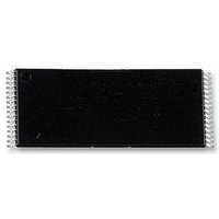
SST49LF008A-33-4C-WHE SILICON STORAGE TECHNOLOGY, SST49LF008A-33-4C-WHE Datasheet - Page 14

SST49LF008A-33-4C-WHE
Manufacturer Part Number
SST49LF008A-33-4C-WHE
Description
MEMORY, FLASH, 8M, SERIAL, 32TSOP
Manufacturer
SILICON STORAGE TECHNOLOGY
Datasheet
1.SST49LF008A-33-4C-WHE.pdf
(42 pages)
Specifications of SST49LF008A-33-4C-WHE
Memory Size
8Mbit
Clock Frequency
33MHz
Supply Voltage Range
3V To 3.6V
Memory Case Style
TSOP
No. Of Pins
32
Operating Temperature Range
0°C To +70°C
Svhc
No SVHC (18-Jun-2010)
Memory Type
Flash
Memory Configuration
1024K X 8
Interface Type
Parallel
Rohs Compliant
Yes
Lead Free Status / RoHS Status
Lead free / RoHS Compliant
Available stocks
Company
Part Number
Manufacturer
Quantity
Price
Part Number:
SST49LF008A-33-4C-WHE
Manufacturer:
SST
Quantity:
20 000
Part Number:
SST49LF008A-33-4C-WHE-T
Manufacturer:
SST
Quantity:
20 000
Data Sheet
Abort Mechanism
If FWH4 is driven low for one or more clock cycles during a
FWH cycle, the cycle will be terminated and the device will
wait for the ABORT command. The host may drive the
FWH[3:0] with ‘1111b’ (ABORT command) to return the
device to Ready mode. If abort occurs during a Write oper-
ation, the data may be incorrectly altered.
Response To Invalid Fields
During FWH operations, the FWH will not explicitly indicate
that it has received invalid field sequences. The response
to specific invalid fields or sequences is as follows:
Address out of range: The FWH address sequence is
7 fields long (28 bits), but only the last five address fields
(20 bits) will be decoded by SST49LF008A.
Address A
writes to the flash core (A
(A
Invalid IMSIZE field: If the FWH receives an invalid size
field during a Read or Write operation, the device will reset
and no operation will be attempted. The SST49LF008A will
not generate any kind of response in this situation. Invalid-
size fields for a Read/Write cycle are anything but 0000b.
Device Memory Hardware Write Protection
The Top Boot Lock (TBL#) and Write Protect (WP#) pins
are provided for hardware write protection of device
memory in the SST49LF008A. The TBL# pin is used to
write protect 16 boot sectors (64 KByte) at the highest
flash memory address range for the SST49LF008A.
WP# pin write protects the remaining sectors in the flash
memory.
An active low signal at the TBL# pin prevents Program and
Erase operations of the top boot sectors. When TBL# pin is
held high, write protection of the top boot sectors is then
determined by the Boot Block Locking register. The WP#
pin serves the same function for the remaining sectors of
the device memory. The TBL# and WP# pins write protec-
tion functions operate independently of one another.
Both TBL# and WP# pins must be set to their required
protection states prior to starting a Program or Erase
operation. A logic level change occurring at the TBL# or
WP# pin during a Program or Erase operation could
cause unpredictable results. TBL# and WP# pins cannot
be left unconnected.
©2006 Silicon Storage Technology, Inc.
22
=0).
22
has the special function of directing reads and
22
=1) or to the register space
14
TBL# is internally OR’ed with the top Boot Block Locking
register. When TBL# is low, the top Boot Block is hard-
ware write protected regardless of the state of the Write-
Lock bit for the Boot Block Locking register. Clearing the
Write-Protect bit in the register when TBL# is low will have
no functional effect, even though the register may indicate
that the block is no longer locked.
WP# is internally OR’ed with the Block Locking register.
When WP# is low, the blocks are hardware write pro-
tected regardless of the state of the Write-Lock bit for the
corresponding Block Locking registers. Clearing the
Write-Protect bit in any register when WP# is low will have
no functional effect, even though the register may indicate
that the block is no longer locked.
Reset
A V
and RST# pins have the same function internally. It is
required to drive INIT# or RST# pins low during a system
reset to ensure proper CPU initialization.
During a Read operation, driving INIT# or RST# pins low
deselects the device and places the output drivers,
FWH[3:0], in a high-impedance state. The reset signal
must be held low for a minimal duration of time T
reset latency will occur if a reset procedure is performed
during a Program or Erase operation. See Table 17, Reset
Timing Parameters for more information. A device reset
during an active Program or Erase will abort the operation
and memory contents may become invalid due to data
being altered or corrupted from an incomplete Erase or
Program operation.
Write Operation Status Detection
The SST49LF008A device provides two software means to
detect the completion of a Write (Program or Erase) cycle,
in order to optimize the system Write cycle time. The soft-
ware detection includes two status bits: Data# Polling
(DQ
mode is incorporated into the FWH Read cycle. The actual
completion of the nonvolatile write is asynchronous with the
system; therefore, either a Data# Polling or Toggle Bit read
may be simultaneous with the completion of the Write
cycle. If this occurs, the system may possibly get an errone-
ous result, i.e., valid data may appear to conflict with either
DQ
erroneous result occurs, the software routine should
include a loop to read the accessed location an additional
two (2) times. If both reads are valid, then the device has
completed the Write cycle, otherwise the rejection is valid.
7
IL
7
) and Toggle Bit (DQ
or DQ
on INIT# or RST# pin initiates a device reset. INIT#
6
. In order to prevent spurious rejection, if an
8 Mbit Firmware Hub
6
). The End-of-Write detection
SST49LF008A
S71161-11-000
RSTP .
3/06
A


